ZHCSDZ3D December 2014 – January 2017
PRODUCTION DATA.
- 1 特性
- 2 应用
- 3 说明
- 4 修订历史记录
- 5 说明 (续)
- 6 Pin Configuration and Functions
-
7 Specifications
- 7.1 Absolute Maximum Ratings
- 7.2 ESD Ratings
- 7.3 Recommended Operating Conditions
- 7.4 Thermal Information
- 7.5 Supply Voltage
- 7.6 Supply Current
- 7.7 Power Supply Control
- 7.8 Low-Voltage General Purpose I/O (TSx)
- 7.9 High-Voltage General Purpose I/O (GPIO0, GPIO1)
- 7.10 AFE Power-On Reset
- 7.11 Internal 1.8-V LDO
- 7.12 Current Wake Comparator
- 7.13 Coulomb Counter
- 7.14 CC Digital Filter
- 7.15 ADC
- 7.16 ADC Digital Filter
- 7.17 ADC Multiplexer
- 7.18 Cell Balancing Support
- 7.19 Cell Detach Detection
- 7.20 Internal Temperature Sensor
- 7.21 NTC Thermistor Measurement Support (ADCx)
- 7.22 High-Frequency Oscillator
- 7.23 Low-Frequency Oscillator
- 7.24 Voltage Reference 1
- 7.25 Voltage Reference 2
- 7.26 Instruction Flash
- 7.27 Data Flash
- 7.28 Current Protection Thresholds
- 7.29 N-CH FET Drive (CHG, DSG)
- 7.30 FUSE Drive (AFEFUSE)
- 7.31 Battery Charger Voltage Regulation (VFB)
- 7.32 Battery Charger Current Sense (HSRP, HSRN)
- 7.33 Battery Charger Precharge Current Sense (HSRP, HSRN)
- 7.34 AC Adapter Fault Detect (HSRN, VCC)
- 7.35 Battery Charger Overcurrent Detection (V)HSRP, (V)HSRN
- 7.36 Battery Charger Undercurrent Detection (V)HSRP, (V)HSRN
- 7.37 System Operation Detection (V)HSRN
- 7.38 Battery Overvoltage Comparator (VFB)
- 7.39 Regulator (REGN)
- 7.40 PWM High-Side Driver (HiDRV)
- 7.41 PWM Low-Side Driver (LoDRV)
- 7.42 PWM Information
- 7.43 Charger Power-Up Sequence
- 7.44 Thermal Shutdown Comparator
- 7.45 SMBus High Voltage I/O
- 7.46 SMBus
- 7.47 SMBus XL
- 7.48 Timing Requirements
- 7.49 Typical Characteristics
-
8 Detailed Description
- 8.1 Overview
- 8.2 Functional Block Diagram
- 8.3 Feature Description
- 9 Application and Implementation
- 10Power Supply Recommendations
- 11Layout
- 12器件和文档支持
- 13机械、封装和可订购信息
9 Application and Implementation
NOTE
Information in the following applications sections is not part of the TI component specification, and TI does not warrant its accuracy or completeness. TI’s customers are responsible for determining suitability of components for their purposes. Customers should validate and test their design implementation to confirm system functionality.
9.1 Application Information
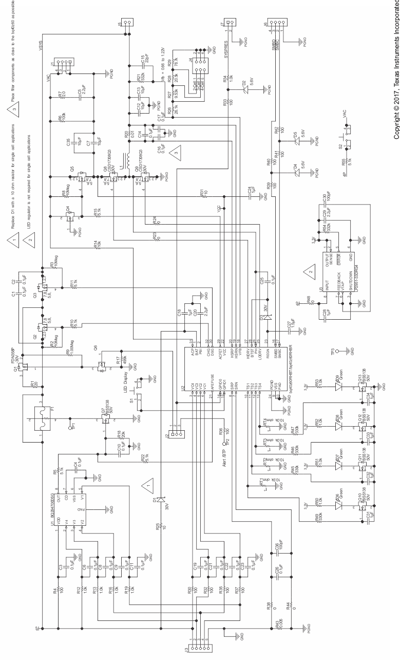
The bq40z60 is a monolithic charger and gas gauge solution for multi-cell battery packs. By integrating these devices, software control can be handed off from the host microcontroller to the gas gauge controller, providing for potential energy savings that correlate to runtime.
9.2 Typical Applications
NOTE
The feedback resistor to VFB from charging output will have different values based on the number of series cells configured for charging the pack.
9.2.1 Design Requirements
For this design example, use the parameters listed in Table 2 as the input parameters.
Table 2. Design Parameters
| Design Parameter | Example Value |
|---|---|
| Input Voltage Range | 15–22 V |
| 3-Cell Battery Voltage Range | 9 V–12.6 V |
| 4-Cell Battery Voltage Range | 12 V–16.8 V |
| Operating Frequency | 1000 kHz |
9.2.2 Detailed Design Procedure
9.2.2.1 Inductor Selection
The bq40z60 has a 1000-kHz switching frequency to allow the use of small inductor and capacitor values. Inductor saturation current should be higher than the charging current (ICHG) plus half the ripple current (IRIPPLE):

The inductor ripple current depends on input voltage (VIN), duty cycle (D = VOUT/VIN), switching frequency (fs) and inductance (L):

The maximum inductor ripple current happens with D = 0.5 or close to 0.5. For example, the battery charging voltage range is from 9 V to 12.6 V for a 3-cell battery pack. For 20-V adaptor voltage, 10-V battery voltage gives the maximum inductor ripple current. Another example is a 4-cell battery: The battery voltage range is from 12 V to 16.8 V, and 12-V battery voltage gives the maximum inductor ripple current.
Usually inductor ripple is designed in the range of (20%–40%) maximum charging current as a trade-off between inductor size and efficiency for a practical design.
The bq40z60 has cycle-by-cycle charge undercurrent protection (UCP) by monitoring the charging-current sensing resistor to prevent negative inductor current. The typical UCP threshold is 5-mV falling edge corresponding to 0.5-A falling edge for a 10-mΩ charging-current sensing resistor.
9.2.2.2 Input Capacitor
The input capacitor should have enough ripple-current rating to absorb input switching ripple current. The worst-case RMS ripple current is half of the charging current when the duty cycle is 0.5. If the converter does not operate at 50% duty cycle, then the worst-case capacitor RMS current ICIN occurs where the duty cycle is closest to 50% and can be estimated using the following equation:

A low-ESR ceramic capacitor such as X7R or X5R is preferred for the input-decoupling capacitor and should be placed to the drain of the high-side MOSFET and source of the low-side MOSFET as close as possible. The voltage rating of the capacitor must be higher than the normal input voltage level. A 25-V or higher-rating capacitor is preferred for 20-V input voltage. 10-µF to 20-µF capacitance is suggested for typical of 3-A to 4-A charging current.
9.2.2.3 Output Capacitor
Output capacitor also should have enough ripple-current rating to absorb the output switching ripple current. The output capacitor RMS current ICOUT is given:

The output capacitor voltage ripple can be calculated as follows:

At a certain input/output voltage and switching frequency, the voltage ripple can be reduced by increasing the output filter LC. The bq40z60 has an internal loop compensator. To get good loop stability, the resonant frequency of the output inductor and output capacitor should be designed between 21 kHz and 27 kHz. The preferred ceramic capacitor has a 25-V or higher rating, X7R or X5R for a 4-cell application.
9.2.2.4 Power MOSFETs Selection
Two external N-CH MOSFETs are used for a synchronous switching battery charger. The gate drivers are internally integrated into the IC with 6 V of gate drive voltage. 30-V or higher voltage rating MOSFETs are preferred for 20-V input voltage, and 40 V or higher-rating MOSFETs are preferred for 20-V to 28-V input voltage.
Figure-of-merit (FOM) is usually used for selecting the proper MOSFET based on a tradeoff between the conduction loss and switching loss. For a top-side MOSFET, FOM is defined as the product of the MOSFET on-resistance, rDS(on), and the gate-to-drain charge, QGD. For a bottom-side MOSFET, FOM is defined as the product of the MOSFET on-resistance, rDS(on), and the total gate charge, QG.

The lower the FOM value, the lower the total power loss. Usually a lower rDS(on) has a higher cost with the same package size.
The top-side MOSFET loss includes conduction loss and switching loss. It is a function of duty cycle (D = VOUT/VIN), charging current (ICHG), the MOSFET on-resistance tDS(on)), input voltage (VIN), switching frequency (fS), turn-on time (ton), and turn-off time (toff):

The first item represents the conduction loss. Usually MOSFET rDS(on) increases by 50% with 100°C junction temperature rise. The second term represents the switching loss. The MOSFET turn-on and turn-off times are given by:

where Qsw is the switching charge, Ion is the turn-on gate-driving current, and Ioff is the turn-off gate driving current. If the switching charge is not given in the MOSFET data sheet, it can be estimated by gate-to-drain charge (QGD) and gate-to-source charge (QGS):

Total gate-driving current can be estimated by the REGN voltage (VREGN), MOSFET plateau voltage (Vplt), total turn-on gate resistance (Ron), and turn-off gate resistance (Roff) of the gate driver:

The conduction loss of the bottom-side MOSFET is calculated with the following equation when it operates in synchronous continuous-conduction mode:

If the HSRP–HSRN voltage decreases below 5 mV (the charger is also forced into non-synchronous mode when the average HSRP–HSRN voltage is lower than 1.7 mV), the low-side FET is turned off for the remainder of the switching cycle to prevent negative inductor current. As a result, all the freewheeling current goes through the body diode of the bottom-side MOSFET. The maximum charging current in non-synchronous mode can be up to 1.6 A (0.5 A typ) for a 10-mΩ charging-current sensing resistor, considering IC tolerance. Choose the bottom-side MOSFET with either an internal Schottky or body diode capable of carrying the maximum non-synchronous mode charging current.
MOSFET gate-driver power loss contributes to the dominant losses on the controller IC when the buck converter is switching. The combined high side and low side MOSFET gate charge, Qg_total, is proportional to the power dissipation of the IC, as shown in Equation 12:

Choosing FETs with a lower Qg_total will reduce power loss.
9.2.2.5 Input Filter Design
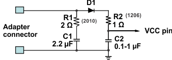
During adaptor hot plug-in, the parasitic inductance and input capacitor from the adaptor cable form a second-order system. The voltage spike at the VCC pin may be beyond the IC maximum voltage rating and damage the IC. The input filter must be carefully designed and tested to prevent an overvoltage event on the VCC pin.
There are several methods for damping or limiting the overvoltage spike during adaptor hot plug-in. An electrolytic capacitor with high ESR as an input capacitor can damp the overvoltage spike well below the IC maximum pin voltage rating. A high-current-capability TVS Zener diode can also limit the overvoltage level to an IC safe level. However, these two solutions may not have low cost or small size.
Figure 9 shows a cost-effective and small size solution. The R1 and C1 are composed of a damping RC network to damp the hot plug-in oscillation. As a result, the overvoltage spike is limited to a safe level. D1 is used for reverse voltage protection for the VCC pin (it can be the body diode of input ACFET). C2 is a VCC pin-decoupling capacitor and it should be placed as close as possible to the VCC pin. R2 and C2 form a damping RC network to further protect the IC from high dv/dt and high-voltage spike. The C2 value should be less than the C1 value so R1 can be dominant over the ESR of C1 to get enough of a damping effect for hot plug-in. The R1 and R2 packages must be sized to handle inrush-current power loss according to the resistor manufacturer’s datasheet. The filter component values always must be verified with the real application, and minor adjustments may be needed to fit in the real application circuit.
 Figure 9. Input Filter
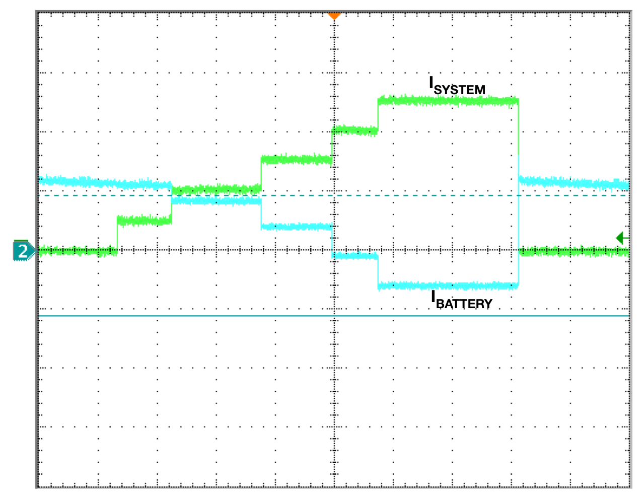
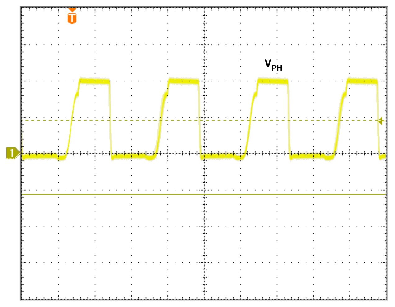
9.2.3 Application Curves

| 1 A/div (on both channels) | ||||
| 4 s/div Timescale | ||||

| 10 V/div | ||||
| 400 ns/div Timescale | ||||
