ZHCSBZ1A December 2013 – December 2014
PRODUCTION DATA.
- 1 特性
- 2 应用
- 3 说明
- 4 修订历史记录
- 5 说明(续)
- 6 Pin Configuration and Functions
-
7 Specifications
- 7.1 Absolute Maximum Ratings
- 7.2 ESD Ratings
- 7.3 Recommended Operating Conditions
- 7.4 Thermal Information
- 7.5 Electrical Characteristics: Supply Current
- 7.6 Electrical Characteristics: Power Supply Control
- 7.7 Electrical Characteristics: AFE Power-On Reset
- 7.8 Electrical Characteristics: AFE Watchdog Reset and Wake Timer
- 7.9 Electrical Characteristics: Current Wake Comparator
- 7.10 Electrical Characteristics: VC1, VC2, VC3, VC4, BAT, PACK
- 7.11 Electrical Characteristics: SMBD, SMBC
- 7.12 Electrical Characteristics: PRES, BTP_INT, DISP
- 7.13 Electrical Characteristics: LEDCNTLA, LEDCNTLB, LEDCNTLC
- 7.14 Electrical Characteristics: Coulomb Counter
- 7.15 Electrical Characteristics: CC Digital Filter
- 7.16 Electrical Characteristics: ADC
- 7.17 Electrical Characteristics: ADC Digital Filter
- 7.18 Electrical Characteristics: CHG, DSG FET Drive
- 7.19 Electrical Characteristics: PCHG FET Drive
- 7.20 Electrical Characteristics: FUSE Drive
- 7.21 Electrical Characteristics: Internal Temperature Sensor
- 7.22 Electrical Characteristics: TS1, TS2, TS3, TS4
- 7.23 Electrical Characteristics: PTC, PTCEN
- 7.24 Electrical Characteristics: Internal 1.8-V LDO
- 7.25 Electrical Characteristics: High-Frequency Oscillator
- 7.26 Electrical Characteristics: Low-Frequency Oscillator
- 7.27 Electrical Characteristics: Voltage Reference 1
- 7.28 Electrical Characteristics: Voltage Reference 2
- 7.29 Electrical Characteristics: Instruction Flash
- 7.30 Electrical Characteristics: Data Flash
- 7.31 Electrical Characteristics: OCD, SCC, SCD1, SCD2 Current Protection Thresholds
- 7.32 Timing Requirements: OCD, SCC, SCD1, SCD2 Current Protection Timing
- 7.33 Timing Requirements: SMBus
- 7.34 Timing Requirements: SMBus XL
- 7.35 Typical Characteristics
-
8 Detailed Description
- 8.1 Overview
- 8.2 Functional Block Diagram
- 8.3
Feature Description
- 8.3.1 Primary (1st Level) Safety Features
- 8.3.2 Secondary (2nd Level) Safety Features
- 8.3.3 Charge Control Features
- 8.3.4 Gas Gauging
- 8.3.5 Configuration
- 8.3.6 Battery Parameter Measurements
- 8.3.7 Battery Trip Point (BTP)
- 8.3.8 Lifetime Data Logging Features
- 8.3.9 Authentication
- 8.3.10 LED Display
- 8.3.11 Voltage
- 8.3.12 Current
- 8.3.13 Temperature
- 8.3.14 Communications
- 8.4 Device Functional Modes
- 9 Applications and Implementation
- 10Power Supply Recommendations
- 11Layout
- 12器件和文档支持
- 13机械封装和可订购信息
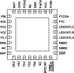
6 Pin Configuration and Functions
RSM Package
32-Pin VQFN with Exposed Thermal Pad
Top View

Pin Functions
| PIN NAME | PIN NUMBER | TYPE(1) | DESCRIPTION |
|---|---|---|---|
| PBI | 1 | P | Power supply backup input pin |
| VC4 | 2 | IA | Sense voltage input pin for most positive cell, and balance current input for most positive cell |
| VC3 | 3 | IA | Sense voltage input pin for second most positive cell, balance current input for second most positive cell, and return balance current for most positive cell |
| VC2 | 4 | IA | Sense voltage input pin for third most positive cell, balance current input for third most positive cell, and return balance current for second most positive cell |
| VC1 | 5 | IA | Sense voltage input pin for least positive cell, balance current input for least positive cell, and return balance current for third most positive cell |
| SRN | 6 | I | Analog input pin connected to the internal coulomb counter peripheral for integrating a small voltage between SRP and SRN where SRP is the top of the sense resistor. |
| NC | 7 | — | Not internally connected. Connect to VSS. |
| SRP | 8 | I | Analog input pin connected to the internal coulomb counter peripheral for integrating a small voltage between SRP and SRN where SRP is the top of the sense resistor. |
| VSS | 9 | P | Device ground |
| TS1 | 10 | IA | Temperature sensor 1 thermistor input pin |
| TS2 | 11 | IA | Temperature sensor 2 thermistor input pin |
| TS3 | 12 | IA | Temperature sensor 3 thermistor input pin |
| TS4 | 13 | IA | Temperature sensor 4 thermistor input pin |
| NC | 14 | — | Not internally connected |
| BTP_INT | 15 | O | Battery Trip Point (BTP) interrupt output |
| PRES or SHUTDN | 16 | I | Host system present input for removable battery pack or emergency system shutdown input for embedded pack |
| DISP | 17 | — | Display control for LEDs |
| SMBD | 18 | I/OD | SMBus data pin |
| SMBC | 19 | I/OD | SMBus clock pin |
| LEDCNTLA | 20 | — | LED display segment that drives the external LEDs depending on the firmware configuration |
| LEDCNTLB | 21 | — | LED display segment that drives the external LEDs depending on the firmware configuration |
| LEDCNTLC | 22 | — | LED display segment that drives the external LEDs depending on the firmware configuration |
| PTC | 23 | IA | Safety PTC thermistor input pin. To disable, connect both PTC and PTCEN to VSS. |
| PTCEN | 24 | IA | Safety PTC thermistor enable input pin. Connect to BAT. To disable, connect both PTC and PTCEN to VSS. |
| FUSE | 25 | O | Fuse drive output pin |
| VCC | 26 | P | Secondary power supply input |
| PACK | 27 | IA | Pack sense input pin |
| DSG | 28 | O | NMOS Discharge FET drive output pin |
| NC | 29 | — | Not internally connected |
| PCHG | 30 | O | PMOS Precharge FET drive output pin |
| CHG | 31 | O | NMOS Charge FET drive output pin |
| BAT | 32 | P | Primary power supply input pin |
(1) P = Power Connection, O = Digital Output, AI = Analog Input, I = Digital Input, I/OD = Digital Input/Output
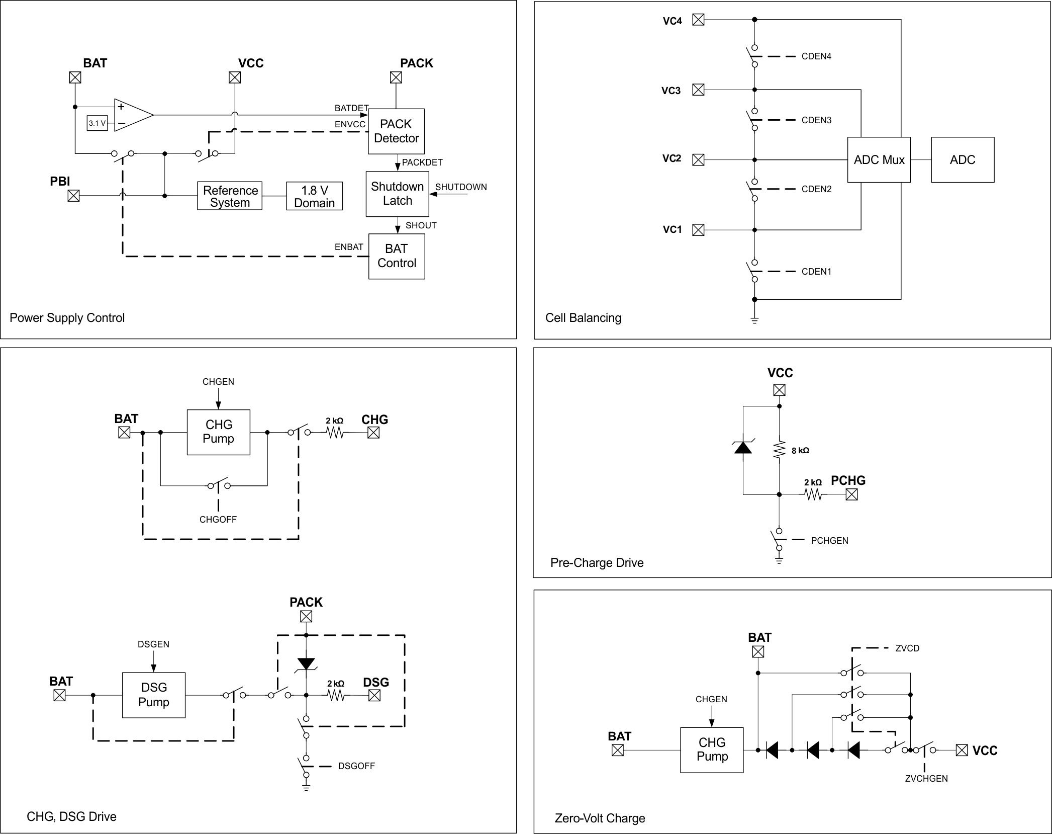
 Figure 1. Pin Equivalent Diagram 1
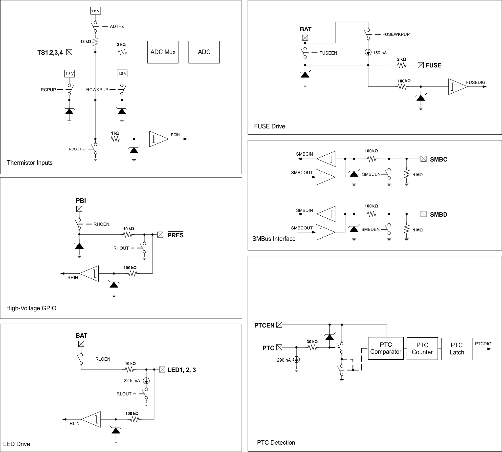
 Figure 2. Pin Equivalent Diagram 2
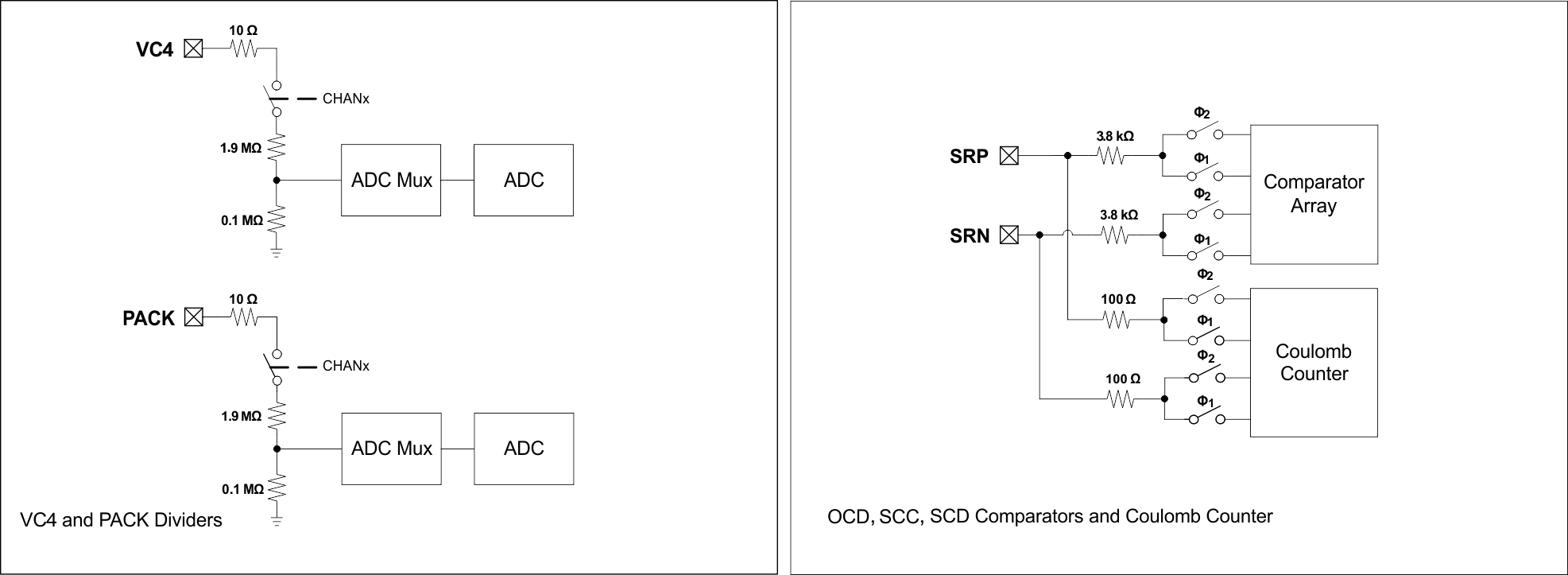
 Figure 3. Pin Equivalent Diagram 3