ZHCSCT0 September 2014
PRODUCTION DATA.
- 1 特性
- 2 应用
- 3 说明
- 4 简化电路原理图
- 5 修订历史记录
- 6 Pin Configuration and Functions
-
7 Specifications
- 7.1 Absolute Maximum Ratings
- 7.2 Handling Ratings
- 7.3 Recommended Operating Conditions
- 7.4 Thermal Information
- 7.5 Supply Current
- 7.6 Digital Input and Output DC Electrical Characteristics
- 7.7 Power-on Reset
- 7.8 2.5-V LDO Regulator
- 7.9 Internal Clock Oscillators
- 7.10 ADC (Temperature and Cell Measurement) Characteristics
- 7.11 Integrating ADC (Coulomb Counter) Characteristics
- 7.12 Data Flash Memory Characteristics
- 7.13 I2C-compatible Interface Communication Timing Characteristics
- 7.14 Typical Characteristics
- 8 Detailed Description
- 9 Application and Implementation
- 10Power Supply Recommendations
- 11Layout
- 12器件和文档支持
- 13机械封装和可订购信息
7 Specifications
7.1 Absolute Maximum Ratings
over operating free-air temperature range (unless otherwise noted)(1)| MIN | MAX | UNIT | ||
|---|---|---|---|---|
| VREGIN | Regulator input range | –0.3 | 5.5 | V |
| –0.3 | 6.0 (2) | V | ||
| VCE | CE input pin | –0.3 | VREGIN + 0.3 | V |
| VCC | Supply voltage range | –0.3 | 2.75 | V |
| VIOD | Open-drain IO pins (SDA, SCL, SOC_INT) | –0.3 | 5.5 | V |
| VBAT | BAT input pin | –0.3 | 5.5 | V |
| –0.3 | 6.0 (2) | V | ||
| VI | Input voltage range to all other pins (BI/TOUT, TS, SRP, SRN, BSCL, BSDA) |
–0.3 | VCC + 0.3 | V |
| TA | Operating free-air temperature range | –40 | 85 | °C |
(1) Stresses beyond those listed as absolute maximum ratings may cause permanent damage to the device. These are stress ratings only, and functional operation of the device at these or any other conditions beyond those indicated as recommended operating conditions is not implied. Exposure to absolute-maximum-rated conditions for extended periods may affect device reliability.
(2) Condition not to exceed 100 hours at 25°C lifetime.
7.2 Handling Ratings
| MIN | MAX | UNIT | |||
|---|---|---|---|---|---|
| Tstg | Storage temperature range | –65 | 150 | °C | |
| V(ESD) | Electrostatic discharge | Human-body model (HBM), per ANSI/ESDA/JEDEC JS-001, BAT pin (1) | 0 | 1.5 | kV |
| Charged device model (CDM), per JEDEC specification JESD22-C101, all other pins(2) | 0 | 2 | |||
(1) JEDEC document JEP155 states that 500-V HBM allows safe manufacturing with a standard ESD control process.
(2) JEDEC document JEP157 states that 250-V CDM allows safe manufacturing with a standard ESD control process.
7.3 Recommended Operating Conditions
TA = –40°C to 85°C, VREGIN = VBAT = 3.6 V (unless otherwise noted)| PARAMETER | TEST CONDITIONS | MIN | NOM | MAX | UNIT | |
|---|---|---|---|---|---|---|
| VREGIN | Supply voltage | No operating restrictions | 2.8 | 4.5 | V | |
| No flash writes | 2.45 | 2.8 | ||||
| CREGIN | External input capacitor for internal LDO between REGIN and VSS | Nominal capacitor values specified. Recommend a 5% ceramic X5R-type capacitor located close to the device. | 0.1 | μF | ||
| CLDO25 | External output capacitor for internal LDO between VCC and VSS | 0.47 | 1 | μF | ||
| tPUCD | Power-up communication delay | 250 | ms | |||
7.4 Thermal Information
| THERMAL METRIC(1) | CSP (15 PINS) |
UNIT | |
|---|---|---|---|
| RθJA | Junction-to-ambient thermal resistance | 70 | °C/W |
| RJC(top) | Junction-to-case (top) thermal resistance | 17 | |
| RθJB | Junction-to-board thermal resistance | 20 | |
| ψJT | Junction-to-top characterization parameter | 1 | |
| ψJB | Junction-to-board characterization parameter | 18 | |
| RθJC(bottom) | Junction-to-case (bottom) thermal resistance | n/a | |
(1) For more information about traditional and new thermal metrics, see the IC Package Thermal Metrics application report, SPRA953.
7.5 Supply Current
TA = 25°C and VREGIN = VBAT = 3.6 V (unless otherwise noted)| PARAMETER | TEST CONDITIONS | MIN | TYP | MAX | UNIT | |
|---|---|---|---|---|---|---|
| ICC(1) | Normal operating-mode current | Fuel gauge in NORMAL mode ILOAD > Sleep current |
118 | μA | ||
| ISLP+(1) | Sleep+ operating-mode current | Fuel gauge in SLEEP+ mode ILOAD < Sleep current |
62 | μA | ||
| ISLP(1) | Low-power storage-mode current | Fuel gauge in SLEEP mode ILOAD < Sleep current |
23 | μA | ||
| IHIB(1) | Hibernate operating-mode current | Fuel gauge in HIBERNATE mode ILOAD < Hibernate current |
8 | μA | ||
(1) Specified by design. Not production tested. Actual supply current consumption will vary slightly depending on firmware operation and dataflash configuration.
7.6 Digital Input and Output DC Electrical Characteristics
TA = –40°C to 85°C, typical values at TA = 25°C and VREGIN = 3.6 V (unless otherwise noted)| PARAMETER | TEST CONDITIONS | MIN | TYP | MAX | UNIT | |
|---|---|---|---|---|---|---|
| VOL | Output voltage, low (SCL, SDA, SOC_INT, BSDA, BSCL) | IOL = 3 mA | 0.4 | V | ||
| VOH(PP) | Output voltage, high (BSDA, BSCL) | IOH = –1 mA | VCC – 0.5 | V | ||
| VOH(OD) | Output voltage, high (SDA, SCL, SOC_INT) | External pullup resistor connected to VCC | VCC – 0.5 | |||
| VIL | Input voltage, low (SDA, SCL) | –0.3 | 0.6 | V | ||
| Input voltage, low (BI/TOUT) | BAT INSERT CHECK MODE active | –0.3 | 0.6 | |||
| VIH | Input voltage, high (SDA, SCL) | 1.2 | V | |||
| Input voltage, high (BI/TOUT) | BAT INSERT CHECK MODE active | 1.2 | VCC + 0.3 | |||
| VIL(CE) | Input voltage, low (CE) | VREGIN = 2.8 to 4.5 V | 0.8 | V | ||
| VIH(CE) | Input voltage, high (CE) | 2.65 | ||||
| Ilkg(1) | Input leakage current (IO pins) | 0.3 | μA | |||
(1) Specified by design. Not production tested.
7.7 Power-on Reset
TA = –40°C to 85°C, typical values at TA = 25°C and VREGIN = 3.6 V (unless otherwise noted)| PARAMETER | MIN | TYP | MAX | UNIT | ||
|---|---|---|---|---|---|---|
| VIT+ | Positive-going battery voltage input at VCC | 2.05 | 2.15 | 2.20 | V | |
| VHYS | Power-on reset hysteresis | 115 | mV | |||
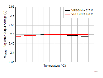
7.8 2.5-V LDO Regulator
TA = –40°C to 85°C, CLDO25 = 1 μF, VREGIN = 3.6 V (unless otherwise noted)| PARAMETER | TEST CONDITIONS | MIN | NOM | MAX | UNIT | |
|---|---|---|---|---|---|---|
| VREG25 | Regulator output voltage (VCC) | 2.8 V ≤ VREGIN ≤ 4.5 V, IOUT ≤ 16 mA(1) | 2.3 | 2.5 | 2.6 | V |
| 2.45 V ≤ VREGIN < 2.8 V (low battery), IOUT ≤ 3 mA |
2.3 | V | ||||
(1) LDO output current, IOUT, is the total load current. LDO regulator should be used to power internal fuel gauge only.
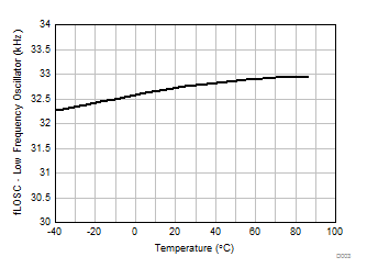
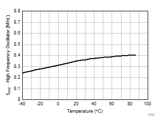
7.9 Internal Clock Oscillators
TA = –40°C to 85°C, 2.4 V < VCC < 2.6 V; typical values at TA = 25°C and VCC = 2.5 V (unless otherwise noted)| PARAMETER | MIN | TYP | MAX | UNIT | ||
|---|---|---|---|---|---|---|
| fOSC | High-frequency oscillator | 8.389 | MHz | |||
| fLOSC | Low-frequency oscillator | 32.768 | kHz | |||
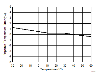
7.10 ADC (Temperature and Cell Measurement) Characteristics
TA = –40°C to 85°C, 2.4 V < VCC < 2.6 V; typical values at TA = 25°C and VCC = 2.5 V (unless otherwise noted)| PARAMETER | TEST CONDITIONS | MIN | TYP | MAX | UNIT | |
|---|---|---|---|---|---|---|
| VADC1 | Input voltage range (TS) | VSS – 0.125 | 2 | V | ||
| VADC2 | Input voltage range (BAT) | VSS – 0.125 | 5 | V | ||
| VIN(ADC) | Input voltage range | 0.05 | 1 | V | ||
| GTEMP | Internal temperature sensor voltage gain | –2 | mV/°C | |||
| tADC_CONV | Conversion time | 125 | ms | |||
| Resolution | 14 | 15 | bits | |||
| VOS(ADC) | Input offset | 1 | mV | |||
| ZADC1(1) | Effective input resistance (TS) | 8 | MΩ | |||
| ZADC2(1) | Effective input resistance (BAT) | Device not measuring cell voltage | 8 | MΩ | ||
| Device measuring cell voltage | 100 | kΩ | ||||
| Ilkg(ADC)(1) | Input leakage current | 0.3 | μA | |||
(1) Specified by design. Not tested in production.
7.11 Integrating ADC (Coulomb Counter) Characteristics
TA = –40°C to 85°C, 2.4 V < VCC < 2.6 V; typical values at TA = 25°C and VCC = 2.5 V (unless otherwise noted)| PARAMETER | TEST CONDITIONS | MIN | TYP | MAX | UNIT | |
|---|---|---|---|---|---|---|
| VSR | Input voltage range, V(SRP) and V(SRN) |
VSR = V(SRP) – V(SRN) | –0.125 | 0.125 | V | |
| tSR_CONV | Conversion time | Single conversion | 1 | s | ||
| Resolution | 14 | 15 | bits | |||
| VOS(SR) | Input offset | 10 | μV | |||
| INL | Integral nonlinearity error | ±0.007 | ±0.034 | % FSR | ||
| ZIN(SR) (1) | Effective input resistance | 2.5 | MΩ | |||
| Ilkg(SR)(1) | Input leakage current | 0.3 | μA | |||
(1) Specified by design. Not tested in production.
7.12 Data Flash Memory Characteristics
TA = –40°C to 85°C, 2.4 V < VCC < 2.6 V; typical values at TA = 25°C and VCC = 2.5 V (unless otherwise noted)| PARAMETER | MIN | TYP | MAX | UNIT | ||
|---|---|---|---|---|---|---|
| tDR(1) | Data retention | 10 | Years | |||
| Flash-programming write cycles(1) | 20,000 | Cycles | ||||
| tWORDPROG(1) | Word programming time | 2 | ms | |||
| ICCPROG(1) | Flash-write supply current | 5 | 10 | mA | ||
| tDFERASE(1) | Data flash master erase time | 200 | ms | |||
| tIFERASE(1) | Instruction flash master erase time | 200 | ms | |||
| tPGERASE(1) | Flash page erase time | 20 | ms | |||
(1) Specified by design. Not production tested
7.13 I2C-compatible Interface Communication Timing Characteristics
TA = –40°C to 85°C, 2.4 V < VCC < 2.6 V; typical values at TA = 25°C and VCC = 2.5 V (unless otherwise noted)| PARAMETER | MIN | TYP | MAX | UNIT | |
|---|---|---|---|---|---|
| tr | SCL or SDA rise time | 300 | ns | ||
| tf | SCL or SDA fall time | 300 | ns | ||
| tw(H) | SCL pulse duration (high) | 600 | ns | ||
| tw(L) | SCL pulse duration (low) | 1.3 | μs | ||
| tsu(STA) | Setup for repeated start | 600 | ns | ||
| td(STA) | Start to first falling edge of SCL | 600 | ns | ||
| tsu(DAT) | Data setup time | 100 | ns | ||
| th(DAT) | Data hold time | 0 | ns | ||
| tsu(STOP) | Setup time for stop | 600 | ns | ||
| t(BUF) | Bus free time between stop and start | 66 | μs | ||
| fSCL | Clock frequency (1) | 400 | kHz | ||
(1) If the clock frequency (fSCL) is > 100 kHz, use 1-byte write commands for proper operation. All other transactions types are supported at 400 kHz (see I2C Interface and I2C Command Waiting Time).
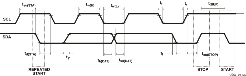 Figure 1. I2C-compatible Interface Timing Diagrams
7.14 Typical Characteristics