ZHCSHR0B September 2017 – September 2019 BQ25910
PRODUCTION DATA.
- 1 特性
- 2 应用
- 3 说明
- 4 修订历史记录
- 5 Pin Configuration and Functions
- 6 Specifications
-
7 Detailed Description
- 7.1 Overview
- 7.2 Functional Block Diagram
- 7.3
Feature Description
- 7.3.1 Device Power-On-Reset (POR)
- 7.3.2 Device Power Up from Battery without Input Source
- 7.3.3 Device Power Up from Input Source
- 7.3.4 Power Up REGN LDO
- 7.3.5 Poor Source Qualification
- 7.3.6 Converter Power-Up
- 7.3.7 Three-Level Buck Converter Theory of Operation
- 7.3.8 Host Mode and Default Mode
- 7.3.9 Battery Charging Management
- 7.3.10 Master Charger and Parallel Charger Interactions
- 7.3.11 Battery Charging Profile
- 7.4 Device Functional Modes
- 7.5 Programming
- 7.6
Register Maps
- 7.6.1
I2C Registers
- 7.6.1.1 Battery Voltage Regulation Limit Register (Address = 0h) [reset = AAh]
- 7.6.1.2 Charger Current Limit Register (Address = 1h) [reset = 46h]
- 7.6.1.3 Input Voltage Limit Register (Address = 2h) [reset = 04h]
- 7.6.1.4 Input Current Limit Register (Address = 3h) [reset = 13h]
- 7.6.1.5 Reserved Register (Address = 4h) [reset = 03h]
- 7.6.1.6 Charger Control 1 Register (Address = 5h) [reset = 9Dh]
- 7.6.1.7 Charger Control 2 Register (Address = 6h) [reset = 33h]
- 7.6.1.8 INT Status Register (Address = 7h) [reset = X]
- 7.6.1.9 FAULT Status Register (Address = 8h) [reset = X]
- 7.6.1.10 INT Flag Status Register (Address = 9h) [reset = 00h]
- 7.6.1.11 FAULT Flag Register (Address = Ah) [reset = 00h]
- 7.6.1.12 INT Mask Register (Address = Bh) [reset = 00h]
- 7.6.1.13 FAULT Mask Register (Address = Ch) [reset = 00h]
- 7.6.1.14 Part Information Register (Address = Dh) [reset = 0Ah]
- 7.6.1
I2C Registers
- 8 Application and Implementation
- 9 Power Supply Recommendations
- 10Layout
- 11器件和文档支持
- 12机械、封装和可订购信息
7.3.8.1 Host Mode and Default Mode in BQ25910
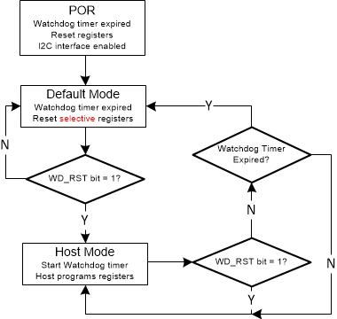
The BQ25910 is a host controlled charger, and will automatically shut off when the I2C watchdog timer is not reset within the timer period. In default (HIZ) mode, the device automatically disables charging until the host writes the EN_CHG bit high again and resets the watchdog timer via the WD_RST bit. When the charger is in default mode, WD_STAT bit is HIGH. When the charger is in host mode, WD_STAT bit is LOW.
After power-on-reset, the device starts in default mode with watchdog timer expired. All the registers are in the default settings. In default mode, the device remains in HIZ mode and will not charge the battery.
Writing a 1 to the WD_RST bit forces the charger out of default mode and into host mode. All the device parameters can be programmed by the host. To keep the device in host mode, the host has to reset the watchdog timer by writing 1 to WD_RST bit before the watchdog timer expires (WD_STAT bit is set), or disable watchdog timer by setting WATCHDOG bits = 00.
When the watchdog timer is expired (WD_STAT bit = 1), the device returns to default mode and registers are reset to default values except as detailed in the I2C register section. As long as the watchdog timer is expired (WD_STAT bit = 1), the device remains in Default Mode without charging the battery, regardless of the EN_CHG bit state. In order to enable charge after watchdog expired, write WD_RST = 1, and EN_CHG = 1.
 Figure 17. Watchdog Timer Flow Chart
 The REG_RST bit can be used to reset all of the registers (except STATUS registers) to their default value at any time.