ZHCSMH4A march   2020  – november 2020 BQ25306

PRODUCTION DATA  

  1.   1
  2. 特性
  3. 应用
  4. 说明
  5. Revision History
  6. 说明(续)
  7. Device Comparison Table
  8. Pin Configuration and Functions
  9. Specifications
    1. 8.1 Absolute Maximum Ratings
    2. 8.2 ESD Ratings
    3. 8.3 Recommended Operating Conditions
    4. 8.4 Thermal Information
    5. 8.5 Electrical Characteristics
    6. 8.6 Timing Requirements
    7. 8.7 Typical Characteristics
  10. Detailed Description
    1. 9.1 Overview
    2. 9.2 Functional Block Diagram
    3. 9.3 Feature Description
      1. 9.3.1 Device Power Up
        1. 9.3.1.1 Power-On-Reset (POR)
        2. 9.3.1.2 REGN Regulator Power Up
        3. 9.3.1.3 Charger Power Up
        4. 9.3.1.4 Charger Enable and Disable by EN Pin
        5. 9.3.1.5 Device Unplugged from Input Source
      2. 9.3.2 Battery Charging Management
        1. 9.3.2.1 Battery Charging Profile
        2. 9.3.2.2 Precharge
        3. 9.3.2.3 Charging Termination
        4. 9.3.2.4 Battery Recharge
        5. 9.3.2.5 Charging Safety Timer
        6. 9.3.2.6 Thermistor Temperature Monitoring
      3. 9.3.3 Charging Status Indicator (STAT)
      4. 9.3.4 Protections
        1. 9.3.4.1 Voltage and Current Monitoring
          1. 9.3.4.1.1 Input Over-Voltage Protection
          2. 9.3.4.1.2 Input Voltage Dynamic Power Management (VINDPM)
          3. 9.3.4.1.3 Input Current Limit
          4. 9.3.4.1.4 Cycle-by-Cycle Current Limit
        2. 9.3.4.2 Thermal Regulation and Thermal Shutdown
        3. 9.3.4.3 Battery Protection
          1. 9.3.4.3.1 Battery Over-Voltage Protection (VBAT_OVP)
          2. 9.3.4.3.2 Battery Short Circuit Protection
        4. 9.3.4.4 ICHG Pin Open and Short Protection
    4. 9.4 Device Functional Modes
      1. 9.4.1 Disable Mode, HiZ Mode, Sleep Mode, Charge Mode, Termination Mode, and Fault Mode
  11. 10Application and Implementation
    1. 10.1 Application Information
    2. 10.2 Typical Applications
      1. 10.2.1 Typical Application
        1. 10.2.1.1 Design Requirements
        2. 10.2.1.2 Detailed Design Procedure
          1. 10.2.1.2.1 Charge Voltage Settings
          2. 10.2.1.2.2 Charge Current Setting
          3. 10.2.1.2.3 Inductor Selection
          4. 10.2.1.2.4 Input Capacitor
          5. 10.2.1.2.5 Output Capacitor
        3. 10.2.1.3 Application Curves
      2. 10.2.2 Typical Application with External Power Path
        1. 10.2.2.1 Design Requirements
      3. 10.2.3 Typical Application with MCU Programmable Charge Current
        1. 10.2.3.1 Design Requirements
  12. 11Power Supply Recommendations
  13. 12Layout
    1. 12.1 Layout Guidelines
    2. 12.2 Layout Example
  14. 13Device and Documentation Support
    1. 13.1 Device Support
      1. 13.1.1 第三方产品免责声明
    2. 13.2 Documentation Support
      1. 13.2.1 Related Documentation
    3. 13.3 接收文档更新通知
    4. 13.4 支持资源
    5. 13.5 Trademarks
    6. 13.6 静电放电警告
    7. 13.7 术语表
  15. 14Mechanical, Packaging, and Orderable Information

封装选项

机械数据 (封装 | 引脚)
散热焊盘机械数据 (封装 | 引脚)

Typical Application with External Power Path

In the case where a system needs to be immediately powered up from VBUS when the battery is overdischarged or dead, the application circuit shown in Figure 10-8 can be used to provide a power path from VBUS/PMID to VSYS. PFET Q4 is an external PFET that turns on to supply VSYS from the battery when VBUS is removed; PFET Q4 turns off when VBUS is plugged in and VSYS is supplied from VBUS/PMID.
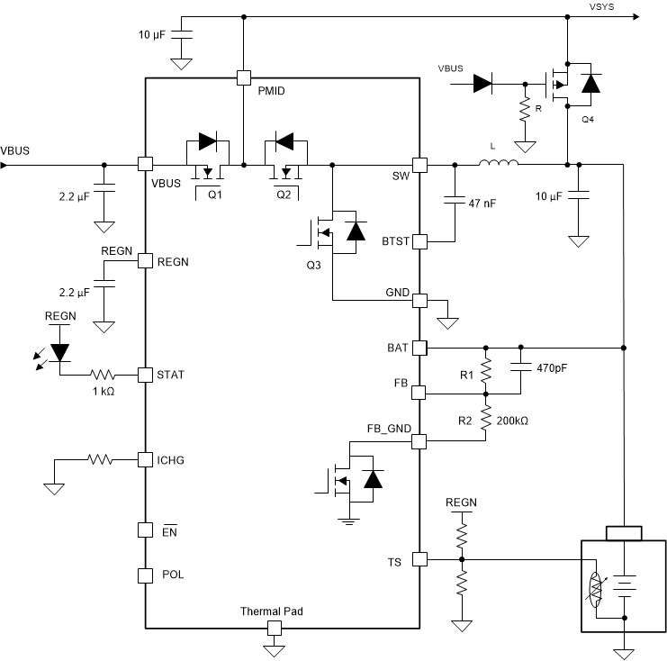
GUID-20201116-CA0I-8J0R-P606-RFGXCS2RQ3DT-low.gif Figure 10-8 Typical Application Diagram with Power Path
(1-µH inductor is recommended if maximum input voltage VVBUS_MAX < 6.2V; 2.2-µH inductor is recommended if maximum input voltage VVBUS_MAX > 6.2V )