SLUSAK9B September 2011 – April 2015
PRODUCTION DATA.
- 1 Features
- 2 Applications
- 3 Description
- 4 Revision History
- 5 Description (continued)
- 6 Pin Configuration and Functions
- 7 Specifications
- 8 Parameter Measurement Information
-
9 Detailed Description
- 9.1 Overview
- 9.2 Functional Block Diagram
- 9.3
Feature Description
- 9.3.1 Adapter Detect and ACOK Output
- 9.3.2 Adapter Overvoltage (ACOVP)
- 9.3.3 System Power Selection
- 9.3.4 Automatic Internal Soft-Start Charger Current
- 9.3.5 Converter Operation
- 9.3.6 Input Overcurrent Protection (ACOC)
- 9.3.7 Charge Overcurrent Protection (CHGOCP)
- 9.3.8 Battery Overvoltage Protection (BATOVP)
- 9.3.9 Battery Shorted to Ground (BATLOWV)
- 9.3.10 Thermal Shutdown Protection (TSHUT)
- 9.3.11 Inductor Short, MOSFET Short Protection
- 9.4 Device Functional Modes
- 9.5 Programming
- 9.6 Register Maps
-
10Application and Implementation
- 10.1 Application Information
- 10.2
Typical Application
- 10.2.1 Design Requirements
- 10.2.2
Detailed Design Procedure
- 10.2.2.1 Negative Output Voltage Protection
- 10.2.2.2 Reverse Input Voltage Protection
- 10.2.2.3 Reduce Battery Quiescent Current
- 10.2.2.4 Inductor Selection
- 10.2.2.5 Input Capacitor
- 10.2.2.6 Output Capacitor
- 10.2.2.7 Power MOSFETs Selection
- 10.2.2.8 Input Filter Design
- 10.2.2.9 bq24735 Design Guideline
- 10.2.3 Application Curves
- 10.3 System Examples
- 11Power Supply Recommendations
- 12Layout
- 13Device and Documentation Support
- 14Mechanical, Packaging, and Orderable Information
10 Application and Implementation
NOTE
Information in the following applications sections is not part of the TI component specification, and TI does not warrant its accuracy or completeness. TI’s customers are responsible for determining suitability of components for their purposes. Customers should validate and test their design implementation to confirm system functionality.
10.1 Application Information
The bq24725A/735EVM-710 evaluation module (EVM) is a complete charger module for evaluating the bq24735. The application curves were taken using the bq24725A/735EVM-710. Refer to the EVM user's guide (SLUU507) for EVM information.
10.2 Typical Application
10.2.1 Design Requirements
For this design example, use the parameters listed in Table 7 as the input parameters.
Table 7. Design Parameters
| DESIGN PARAMETER | EXAMPLE VALUE |
|---|---|
| Input Voltage(2) | 17.7 V < Adapter Voltage < 24 V |
| Input Current Limit (2) | 3.2 A for 65-W adapter |
| Battery Charge Voltage(1) | 12592 mV for 3-s battery |
| Battery Charge Current(1) | 4096 mA for 3-s battery |
| Battery Discharge Current(1) | 6144 mA for 3-s battery |
10.2.2 Detailed Design Procedure
10.2.2.1 Negative Output Voltage Protection
If the battery pack is inserted in reverse order into the charger, output during production or hard shorts on battery-to-ground generates negative output voltage on the SRP and SRN pins. IC internal electrostatic-discharge (ESD) diodes from the GND pin to the SRP or SRN pins and two anti-parallel (AP) diodes between the SRP and SRN pins can be forward-biased and negative current can pass through the ESD diodes and AP diodes when output has negative voltage. Insert two small resistors for SRP and SRN pins to limit the negative current level when output has negative voltage. Suggested resistor value is 10 Ω for the SRP pin and 7 to 8 Ω for the SRN pin. After adding small resistors, the suggested precharge current is at least 192 mA for a 10-mΩ current-sensing resistor. Another method is using a small diode parallel with output capacitor; when battery connection is reversed, the diode turns on and limits the negative voltage level. Using diode protection method without insertion of small resistors into the SRP and SRN pins can get the best charging current accuracy.
10.2.2.2 Reverse Input Voltage Protection
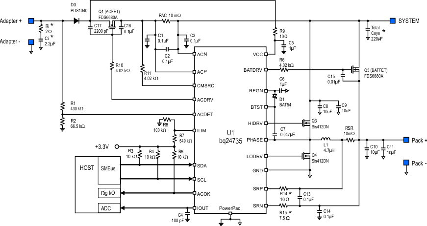
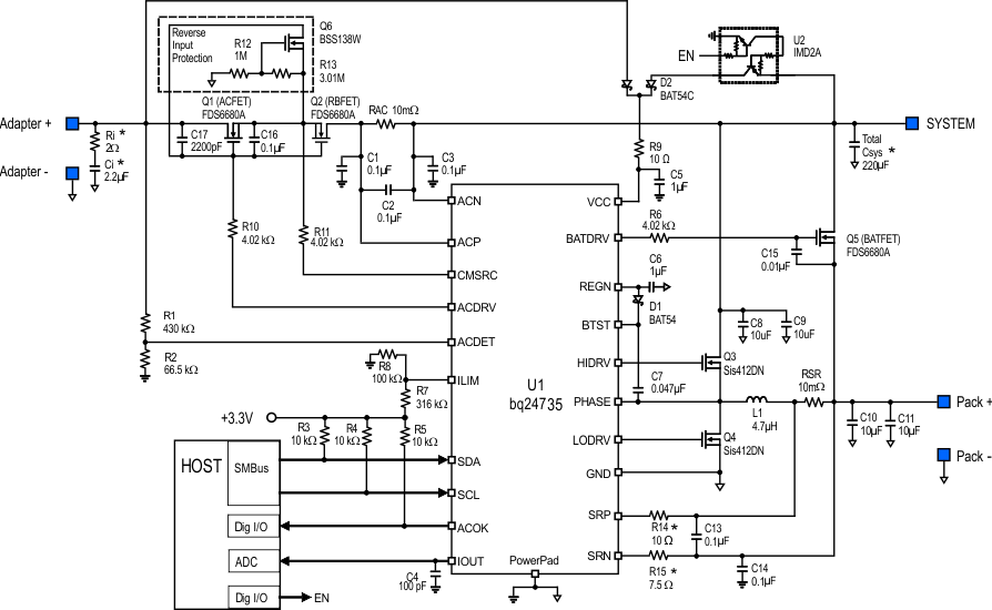
Q6, R12 and R13 in Figure 16 gives system and IC protection from reversed adapter voltage. In normal operation, Q6 is turned off by negative Vgs. When adapter voltage is reversed, Q6 Vgs is positive. As a result, Q6 turns on to short gate and source of Q2 so that Q2 is off. Q2 body diode blocks negative voltage to system. However, CMSRC and ACDRV pins need R10 and R11 to limit the current due to the ESD diode of these pins when turned on. Q6 must has low Vgs threshold voltage and low Qgs gate charge, so it turns on before Q2 turns on. R10 and R11 must have enough power rating for the power dissipation when the ESD diode is on. In Figure 21, the Schottky diode D3 gives the reverse adapter voltage protection, no extra small MOSFET and resistors are needed.
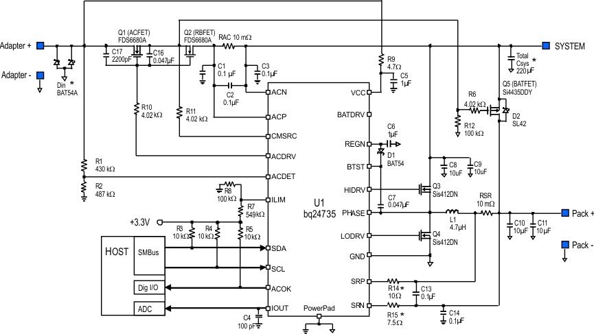
In Figure 22, the Schottky diode Din is used for the reverse adapter voltage protection.
10.2.2.3 Reduce Battery Quiescent Current
When the adapter is not present, if VCC is powered with voltage higher than UVLO directly or indirectly (such as through a LDO or switching converter) from battery, the internal BATFET charge pump gives the BATFET pin 6 V higher voltage than the SRN pin to drive the N-channel BATFET. As a result, the battery has higher quiescent current. This is only necessary when the battery powers the system due to a high system current that goes through the MOSFET channel instead of the body diode to reduce conduction loss and extend the battery working life. When the system is totally shut down, it is not necessary to let the internal BATFET charge pump work. The host controller can use a digital signal EN to disconnect the battery power path to the VCC pin by U2 in Figure 16. As a result, battery quiescent current can be minimized. The host controller still can get power from BATFET body diode because the total system current is the lowest when the system is shut down, so there is no high conduction loss of the body diode.
10.2.2.4 Inductor Selection
The bq24735 has three selectable fixed switching frequencies. Higher switching frequency allows the use of smaller inductor and capacitor values. Inductor saturation current should be higher than the charging current (ICHG) plus half the ripple current (IRIPPLE):

The inductor ripple current depends on input voltage (VIN), duty cycle (D = VOUT/VIN), switching frequency (fS) and inductance (L):

The maximum inductor ripple current happens with D = 0.5 or close to 0.5. For example, the battery charging voltage range is from 9 V to 12.6 V for a 3-cell battery pack. For 20-V adapter voltage, a 10-V battery voltage gives the maximum inductor ripple current. Another example is a 4-cell battery. The battery voltage range is from 12 V to 16.8 V, and 12-V battery voltage gives the maximum inductor ripple current.
Usually, inductor ripple is designed in the range of (20% to 40%) maximum charging current as a trade-off between inductor size and efficiency for a practical design.
The bq24735 has charge undercurrent protection (UCP) by monitoring charging current-sensing resistor cycle-by-cycle. The typical cycle-by-cycle UCP threshold is 5-mV falling edge corresponding to 0.5-A falling edge for a 10-mΩ charging current sensing resistor. When the average charging current is less than 125 mA for a 10-mΩ charging current-sensing resistor, the low-side MOSFET is off until BTST capacitor voltage must refresh the charge. As a result, the converter relies on low-side MOSFET body diode for the inductor freewheeling current.
10.2.2.5 Input Capacitor
Input capacitor should have enough ripple current rating to absorb input switching ripple current. The worst-case RMS ripple current is half of the charging current when duty cycle is 0.5. If the converter does not operate at 50% duty cycle, then the worst-case capacitor RMS current occurs where the duty cycle is closest to 50% and can be estimated by Equation 6:

Low ESR ceramic capacitor such as X7R or X5R is preferred for input decoupling capacitor and should be placed to the drain of the high-side MOSFET and source of the low-side MOSFET as close as possible. Voltage rating of the capacitor must be higher than normal input voltage level. 25-V rating or higher capacitor is preferred for 19- to 20-V input voltage. 10- to 20-μF capacitance is suggested for typical of 3- to 4-A charging current.
Ceramic capacitors show a DC-bias effect. This effect reduces the effective capacitance when a DC-bias voltage is applied across a ceramic capacitor, as on the input capacitor of a charger. The effect may lead to a significant capacitance drop, especially for high input voltages and small capacitor packages. See the manufacturer's data sheet about the performance with a DC-bias voltage applied. It may be necessary to choose a higher voltage rating or nominal capacitance value in order to get the required value at the operating point.
10.2.2.6 Output Capacitor
Output capacitor also should have enough ripple current rating to absorb output switching ripple current. The output capacitor RMS current is given:

The bq24735 has internal loop compensator. To get good loop stability, the resonant frequency of the output inductor and output capacitor should be designed between 10 kHz and 20 kHz. The preferred ceramic capacitor is a 25-V X7R or X5R for output capacitor. A capacitance of 10 to 20 µF is suggested for a typical of 3- to 4-A charging current. Place the capacitors after charging current-sensing resistor to get the best charge current regulation accuracy.
Ceramic capacitors show a DC-bias effect. This effect reduces the effective capacitance when a DC-bias voltage is applied across a ceramic capacitor, as on the output capacitor of a charger. The effect may lead to a significant capacitance drop, especially for high output voltages and small capacitor packages. See the manufacturer's data sheet about the performance with a DC-bias voltage applied. It may be necessary to choose a higher voltage rating or nominal capacitance value in order to get the required value at the operating point.
10.2.2.7 Power MOSFETs Selection
Two external N-channel MOSFETs are used for a synchronous switching battery charger. The gate drivers are internally integrated into the IC with 6 V of gate drive voltage. A 30-V or higher voltage rating MOSFETs are preferred for 19- to 20-V input voltage.
Figure-of-merit (FOM) is usually used for selecting proper MOSFET based on a tradeoff between the conduction loss and switching loss. For the top-side MOSFET, FOM is defined as the product of a MOSFET ON-resistance, RDS(ON), and the gate-to-drain charge, QGD. For the bottom-side MOSFET, FOM is defined as the product of the MOSFET ON-resistance, RDS(ON), and the total gate charge, QG.
The lower the FOM value, the lower the total power loss. Usually lower RDS(ON) has higher cost with the same package size.
The top-side MOSFET loss includes conduction loss and switching loss. It is a function of duty cycle (D=VOUT/VIN), charging current (ICHG), MOSFET ON-resistance (RDS(ON)), input voltage (VIN), switching frequency (fS), turnon time (ton) and turnoff time (toff):

The first item represents the conduction loss. Usually MOSFET RDS(ON) increases by 50% with 100°C junction temperature rise. The second term represents the switching loss. The MOSFET turnon and turnoff times are given by:

where Qsw is the switching charge, Ion is the turnon gate driving current and Ioff is the turnoff gate driving current. If the switching charge is not given in MOSFET data sheet, it can be estimated by gate-to-drain charge (QGD) and gate-to-source charge (QGS):

Gate driving current can be estimated by REGN voltage (VREGN), MOSFET plateau voltage (Vplt), total turnon gate resistance (Ron) and turnoff gate resistance (Roff) of the gate driver:

The conduction loss of the bottom-side MOSFET is calculated with the following equation when it operates in synchronous continuous conduction mode:
When charger operates in nonsynchronous mode, the bottom-side MOSFET is off. As a result all the freewheeling current goes through the body-diode of the bottom-side MOSFET. The body diode power loss depends on its forward voltage drop (VF), nonsynchronous mode charging current (INONSYNC), and duty cycle (D).
The maximum charging current in nonsynchronous mode can be up to 0.25 A for a 10-mΩ charging current sensing resistor, or 0.5 A if battery voltage is below 2.5 V. The minimum duty cycle happens at lowest battery voltage. Choose the bottom-side MOSFET with either an internal Schottky or body diode capable of carrying the maximum nonsynchronous mode charging current.
10.2.2.8 Input Filter Design
During adapter hot plug-in, the parasitic inductance and input capacitor from the adapter cable form a second order system. The voltage spike at VCC pin maybe beyond IC maximum voltage rating and damage IC. The input filter must be carefully designed and tested to prevent overvoltage event on VCC pin.
There are several methods of damping or limiting the overvoltage spike during adapter hot plug-in. An electrolytic capacitor with high ESR as an input capacitor can damp the overvoltage spike well below the IC maximum pin voltage rating. A high current capability TVS Zener diode can also limit the overvoltage level to an IC safe level. However, these two solutions may not have low cost or small size.
A cost-effective and small-size solution is shown in Figure 17. R1 and C1 are composed of a damping RC network to damp the hot plug-in oscillation. As a result the overvoltage spike is limited to a safe level. D1 is used for reverse voltage protection for VCC pin. C2 is VCC pin decoupling capacitor and it should be place to VCC pin as close as possible. C2 value should be less than C1 value so R1 can dominant the equivalent ESR value to get enough damping effect. R2 is used to limit inrush current of D1 to prevent D1 getting damage when adapter hot plug-in. R2 and C2 should have 10-us time constant to limit the DV/DT on VCC pin to reduce inrush current when adapter hot plug in. R1 has high inrush current. R1 package must be sized enough to handle inrush current power loss according to resistor manufacturer’s data sheet. The filter components value always must be verified with real application and minor adjustments may need to fit in the real application circuit.
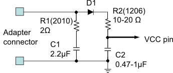 Figure 17. Input Filter
10.2.2.9 bq24735 Design Guideline
The bq24735 has a unique short-circuit protection feature. Its cycle-by-cycle current monitoring feature is achieved through monitoring the voltage drop across RDS(on) of the MOSFETs after a certain amount of blanking time. For a MOSFET short or inductor short circuit, the overcurrent condition is sensed by two comparators, and two counters are triggered. After seven occurrences of a short-circuit event, the charger will be latched off. To reset the charger from latch-off status, reconnect the adapter. Figure 18 shows the bq24735 short-circuit protection block diagram.
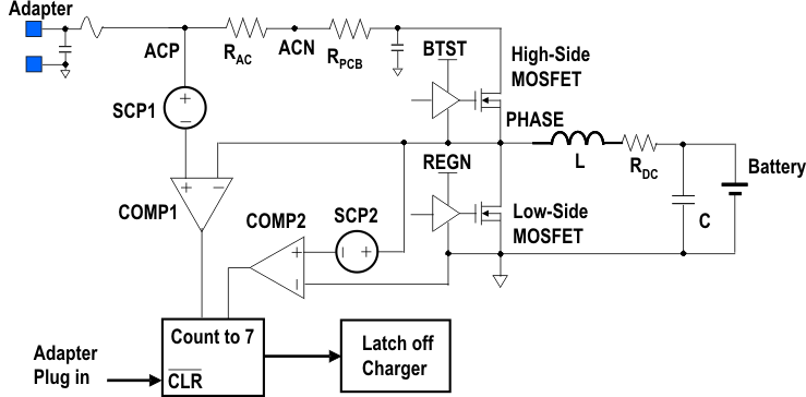 Figure 18. Block Diagram of bq24735 Short-Circuit Protection
In normal operation, the low-side MOSFET current is from source to drain which generates a negative voltage drop when it turns on. As a result, the overcurrent comparator cannot be triggered. When the high-side switch short circuit or inductor short circuit occurs, the large current of the low-side MOSFET is from drain to source and can trigger the low-side switch overcurrent comparator. bq24735 senses the low-side switch voltage drop through the PHASE pin and the GND pin.
The high-side FET short is detected by monitoring the voltage drop between ACP and PHASE. As a result, it not only monitors the high-side switch voltage drop, but also the adapter-sensing resistor voltage drop and PCB trace voltage drop from the ACN terminal of RAC to the charger high-side switch drain. Usually, there is a long trance between input-sensing resistor and charger-converting input, a careful layout will minimize the trace effect.
Table 8. Component List for Typical System Circuit of Figure 16
| PART DESIGNATOR | QTY | DESCRIPTION |
|---|---|---|
| C1, C2, C3, C13, C14, C16 | 6 | Capacitor, Ceramic, 0.1 µF, 25 V, 10%, X7R, 0603 |
| C4 | 1 | Capacitor, Ceramic, 100 pF, 25 V, 10%, X7R, 0603 |
| C5, C6 | 2 | Capacitor, Ceramic, 1 µF, 25 V, 10%, X7R, 0603 |
| C7 | 1 | Capacitor, Ceramic, 0.047 µF, 25 V, 10%, X7R, 0603 |
| C8, C9, C10, C11 | 4 | Capacitor, Ceramic, 10 µF, 25 V, 10%, X7R, 1206 |
| C15 | 1 | Capacitor, Ceramic, 0.01 µF, 25 V, 10%, X7R, 0603 |
| C17 | 1 | Capacitor, Ceramic, 2200 pF, 25 V, 10%, X7R, 0603 |
| Ci | 1 | Capacitor, Ceramic, 2.2 µF, 25 V, 10%, X7R, 1210 |
| Csys | 1 | Capacitor, Electrolytic, 220 µF, 25 V |
| D1 | 1 | Diode, Schottky, 30 V, 200 mA, SOT-23, Fairchild, BAT54 |
| D2 | 1 | Diode, Dual Schottky, 30 V, 200 mA, SOT-23, Fairchild, BAT54C |
| Q1, Q2, Q5 | 3 | N-channel MOSFET, 30 V, 12.5 A, SO-8, Fairchild, FDS6680A |
| Q3, Q4 | 2 | N-channel MOSFET, 30 V, 12 A, PowerPAK 1212-8, Vishay Siliconix, SiS412DN |
| Q6 | 1 | N-channel MOSFET, 50 V, 0.2 A, SOT-323, Diodes, BSS138W |
| L1 | 1 | Inductor, SMT, 4.7 µH, 5.5 A, Vishay Dale, IHLP2525CZER4R7M01 |
| R1 | 1 | Resistor, Chip, 430 kΩ, 1/10 W, 1%, 0603 |
| R2 | 1 | Resistor, Chip, 66.5 kΩ, 1/10 W, 1%, 0603 |
| R3, R4, R5 | 3 | Resistor, Chip, 10 kΩ, 1/10 W, 1%, 0603 |
| R6, R10, R11 | 3 | Resistor, Chip, 4.02 kΩ, 1/10 W, 1%, 0603 |
| R7 | 1 | Resistor, Chip, 316 kΩ, 1/10 W, 1%, 0603 |
| R8 | 1 | Resistor, Chip, 100 kΩ, 1/10 W, 1%, 0603 |
| R9 | 1 | Resistor, Chip, 10 Ω, 1/4 W, 1%, 1206 |
| R12 | 1 | Resistor, Chip, 1.00 MΩ, 1/10 W, 1%, 0603 |
| R13 | 1 | Resistor, Chip, 3.01 MΩ, 1/10 W, 1%, 0603 |
| R14 | 1 | Resistor, Chip, 10 Ω, 1/10 W, 5%, 0603 |
| R15 | 1 | Resistor, Chip, 7.5 Ω, 1/10 W, 5%, 0603 |
| RAC, RSR | 2 | Resistor, Chip, 0.01 Ω, 1/2 W, 1%, 1206 |
| Ri | 1 | Resistor, Chip, 2 Ω, 1/2 W, 1%, 1210 |
| U1 | 1 | Charger controller, 20-pin VQFN, TI, bq24735RGR |
| U2 | 1 | Dual digital transistor, 40 V, 30 mA, SC-74, Rohm, IMD2A |
10.2.3 Application Curves
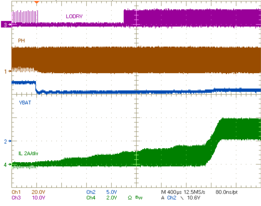
| CH1: PHASE, 20 V/div, | CH2: battery voltage, 5 V/div, | |
| CH3: LODRV, 10 V/div, | ||
| CH4: inductor current, 2 A/div, 400 µs/div | ||
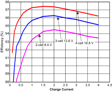
| VIN = 20 V | FS = 750 kHz | L = 4.7 µH |
10.3 System Examples
