ZHCSCR4F June 2014 – August 2015
UNLESS OTHERWISE NOTED, this document contains PRODUCTION DATA.
- 1 特性
- 2 应用范围
- 3 说明
- 4 修订历史记录
- 5 Pin Configuration and Functions
- 6 Specifications
-
7 Detailed Description
- 7.1 Overview
- 7.2 Functional Block Diagram
- 7.3 Feature Description
- 7.4
Device Functional Modes
- 7.4.1 High Impedance Mode
- 7.4.2 Battery Only Connected
- 7.4.3 Input Connected
- 7.4.4 Battery Charging Process
- 7.4.5 Charge Time Optimizer
- 7.4.6 Battery Detection
- 7.4.7 Battery Overvoltage Protection (BOVP)
- 7.4.8 Dynamic Power Path Management
- 7.4.9 Battery Discharge FET (BGATE)
- 7.4.10 IUSB1, IUSB2, and IUSB3 Input
- 7.4.11 Safety Timer in Charge Mode
- 7.4.12 LDO Output (DRV)
- 7.4.13 External NTC Monitoring (TS)
- 7.4.14 Thermal Regulation and Protection
- 7.4.15 Status Outputs (CHG, PG)
- 7.4.16 Boost Mode Operation
- 8 Applications and Implementation
- 9 Power Supply Recommendations
- 10Layout
- 11器件和文档支持
- 12机械、封装和可订购信息
7 Detailed Description
7.1 Overview
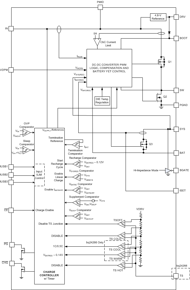
The bq24266 is a highly integrated single cell Li-Ion battery charger and system power path management devices targeted for space-limited, portable applications with high capacity batteries. The single cell charger has a single input that supports operation from either a USB port or wall adapter supply for a versatile solution.
The power path management feature allows the bq24266 to power the system from a high efficiency DC to DC converter while simultaneously and independently charging the battery. The charger monitors the battery current at all times and reduces the charge current when the system load requires current above the input current limit or the adapter cannot support the required load, causing the adapter voltage to fall (VIN_DPM). This allows for proper charge termination and timer operation. The system voltage is regulated to the battery voltage but will not drop below 3.5V (VMINSYS). This minimum system voltage support enables the system to run with a defective or absent battery pack and enables instant system turn-on even with a totally discharged battery or no battery. The power-path management architecture also permits the battery to supplement the system current requirements when the adapter cannot deliver the peak system currents. The power-path feature coupled with VIN-DPM, enables the use of many adapters with no hardware change. The charge parameters are programmable using the ISET pin. To support USB OTG applications, the bq24266 is configurable to boost the battery voltage to 5V at the input. In this mode, the bq24266 supplies up to 1A and operates with battery voltages down to 3.3V.
The battery is charged using a standard Li-Ion charge profile with three phases: precharge, constant current and constant voltage. In all charge phases, an internal control loop monitors the IC junction temperature and reduces the input current to prevent the junction temperature from rising above 125°C. With the bq24266 a voltage-based, JEITA compatible battery pack thermistor monitoring input (TS) is included that monitors battery temperature and automatically changes charge parameters to prevent the battery from charging outside of its safe temperature range.
7.2 Functional Block Diagram
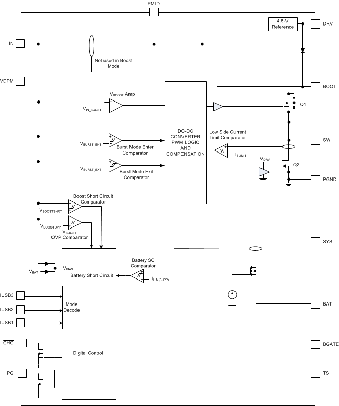 Figure 8. Block Diagram in Boost Mode
7.3 Feature Description
The bq24266 is a highly integrated single cell Li-Ion battery charger and system power path management devices that supports operation from either a USB port or wall adapter supply. The power path feature allows the bq24266 to power the system from a high efficiency DC to DC converter while simultaneously and independently charging the battery. The power path also permits the battery to supplement the system current requirements when the adapter cannot. Many features are programmable using dedicated pins. To support USB OTG applications, the bq24266 is configurable to boost the battery voltage to 5V and supply up to 1A at the input. The battery is charged with three phases: precharge, constant current and constant voltage. Thermal regulation prevents the die temperature from exceeding 125°C. With the bq24266, a JEITA compatible battery pack thermistor monitoring input (TS) is included to prevent the battery from charging outside of its safe temperature range.
7.4 Device Functional Modes
7.4.1 High Impedance Mode
High Impedance mode (Hi-Z mode) is the low quiescent current state for the bq24266. During Hi-Z mode, the buck converter is off, and the battery FET and BGATE are on. SYS is powered by BAT. The bq24266 is in Hi-Z mode when VIN < VUVLO or the IUSB1, IUSB2, and IUSB3 pins are all driven high. Hi-Z mode resets the safety timer. When exiting Hi-Z mode, charging resumes in approximately 110ms.
7.4.2 Battery Only Connected
When the battery is connected with no input source, the battery FET is turned on. After the battery rises above VBATUVLO and the deglitch time, tDGL(BAT), the SYS output starts to rise. In this mode, the current is not regulated; however, there is a short circuit current limit. If the short circuit limit (ILIM(DISCHG)) is reached for the deglitch time (tDGL(SC)), the battery FET is turned off for the recovery time (tREC(SC)). After the recovery time, the battery FET is turned on to test and see if the short has been removed. If it has not, the FET turns off and the process repeats until the short is removed. This process protects the internal FET from over current. If an external FET is used for discharge, the body diode prevents the load on SYS from being disconnected from the battery and tDGL(BAT) is not applicable.
7.4.3 Input Connected
7.4.3.1 Input Voltage Protection in Charge Mode
7.4.3.1.1 Sleep Mode
The bq24266 enters the low-power sleep mode if the voltage on VIN falls below sleep-mode entry threshold, VBAT+VSLP, and VIN is higher than the undervoltage lockout threshold, VUVLO. In sleep mode, the input is isolated from the battery. This feature prevents draining the battery during the absence of VIN. When VIN < VBAT+ VSLP, the bq24266 turns off the PWM converter and turns the battery FET and BGATE on. Once VIN > VBAT+ VSLP, the device initiates a new charge cycle.
7.4.3.1.2 Input Voltage Based Dynamic Power Management (VIN-DPM)
During normal charging process, if the input power source is not able to support the programmed or default charging current, the supply voltage deceases. Also, at higher currents, large input line impedances may cause the voltage at the device to droop. Once the supply drops to VIN_DPM (default 4.2V), the charge current limit is reduced to prevent the further drop of the supply. When the IC enters this mode, the charge current is lower than the set value. This feature ensures IC compatibility with adapters with different current capabilities without a hardware change. Figure 9 shows the VIN-DPM behavior to a current limited source. In this figure the input source has a 2A current limit and the device is charging at 1A. A 2.5A load transient then occurs on VSYS causing the adapter to hit its current limit and collapse, while VSYS goes from VSYSREG(LO) to VMINSYS. The safety timer is extended while VIN-DPM is active. Additionally, termination is disabled.
The VINDPM threshold for the adapter modes (1.5A and 2.5A) is set using a resistor divider with VDPM connected to the center tap. Select 10kΩ for the bottom resistor. The top resistor is selected using equation Equation 1.
Where VIN_DPM is the desired VIN_DPM threshold and VDPM is the regulation threshold at the pin specified in the Electrical Characteristics table.

.
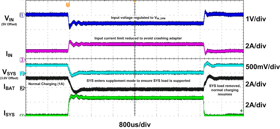 Figure 9. bq24266 VIN-DPM
7.4.3.1.3 Input Overvoltage Protection
The built-in input overvoltage protection protects the bq24266 and downstream components connected to SYS and/or BAT against damage from overvoltage on the input supply (Voltage from VIN to PGND). When VIN > VOVP, the bq24266 turns off the PWM converter immediately. After the deglitch time tDGL(BUCK_OVP), an OVP fault is determined to exist. During the OVP fault the bq24266 turns the battery FET and BGATE on. Once the OVP fault is removed, the device returns to normal operation.
The OVP threshold is 14V for operation from standard adapters and from 12V sources.
7.4.3.2 Charge Profile
When a valid input source is connected (VIN>VUVLO and VBAT+VSLP<VIN<VOVP), charging is enabled.
The charge current, ICHARGE, is set using the ISET pin by connecting a resistor form ISET to GND. The current is programmable from 500mA to 3A using Equation 2, where ICHARGE is in Amperes, and KISET is the value specified in the Electrical Characteristics table.

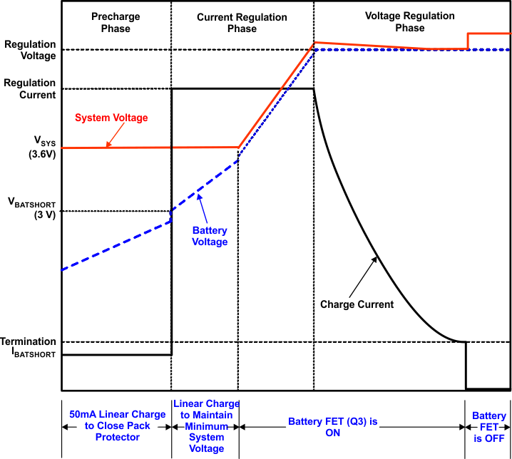
The bq24266 supports a precision Li-Ion or Li-Polymer charging system for single-cell applications. Charging is done through the internal battery MOSFET. There are 6 loops that influence the charge current; constant current loop (CC), constant voltage loop (CV), thermal regulation loop, minimum system voltage loop (MINSYS), input current limit and VIN-DPM. During the charging process, all six loops are enabled and the one that is dominant takes control. The minimum system output feature regulates the system voltage to VSYSREG(LO), so that startup is enabled even for a missing or deeply discharged battery. Figure 10 shows a typical charge profile including the minimum system output voltage feature.
7.4.4 Battery Charging Process
When the battery is deeply discharged or shorted, the bq24266 applies a IBATSHRT current to close the battery protector switch and bring the battery voltage up to acceptable charging levels. During this time, the battery FET is off and the system output is regulated to VSYSREG(LO). Once the battery rises above VBATSHRT, the charge current is regulated to the value set by ISET. The battery FET is linearly regulated to maintain the system voltage at VSYSREG(LO). Under normal conditions, the time spent in this region is a very short percentage of the total charging time, so the linear regulation of the charge current does not affect the overall charging efficiency for very long. If the die temperature does heat up, the thermal regulation loop reduces the input current to maintain a die temperature at 125°C. If the current limit for the SYS output is reached (limited by the input current limit, VIN-DPM, or 100% duty cycle), the SYS output drops to the VMINSYS output voltage. When this happens, the charge current is reduced to ensure the system is supplied with all the current that is needed while maintaining the minimum system voltage. If the charge current is reduced to 0mA, pulling further current from SYS causes the output to fall to the battery voltage and enter supplement mode (see the “Dynamic Power Path Management” section for more details).
Once the battery is charged enough that the system voltage rises above VSYSREG(LO) (approximately 3.5V), the battery FET is turned on fully and the battery is charged with the full programmed charge current set by ISET. The charge current is regulated to ICHARGE until the voltage between BAT and PGND reaches the regulation voltage. The voltage between BAT and PGND is regulated to VBATREG (CV mode) while the charge current naturally tapers down as shown in Figure 10. During CV mode, the SYS output remains connected to the battery. The impedance of the battery FET is increased to 4x of the fully on value when IBAT falls below ~350mA to provide increased accuracy during termination. This will show a small rise in the SYS voltage when the RDS(ON) increases below ~350mA.
Once the charge current tapers down to the termination threshold, ITERM, and the battery voltage is above the recharge threshold, the bq24266 terminates charge, turns off the battery charging FET and enters battery detection (see Battery Detection section for more details). The system output is regulated to the VSYSREG(HI) and supports the full current available from the input. The battery supplement mode is available to supply any SYS load that cannot be supported by the input source (see the Dynamic Power Path Management section for more details). The termination current level is set to 10% of the charge current. Termination is disabled when any loop is active other than CC or CV. This includes VINDPM, input current limit, or thermal regulation. Termination is also disabled during TS warm/cool conditions.
A charge cycle is initiated when one of the following conditions is detected:
- The battery voltage falls below the VBATREG-VRCH threshold.
- IN Power-on reset (POR)
- Charge disabled then enabled using CE
- IUSB toggeld from high impedance to any charge state
7.4.5 Charge Time Optimizer
The CC to CV transition is enhanced in the bq24266 architecture. The "knee" between CC and CV is very sharp. This enables the charger to remain in CC mode as long as possible before beginning to taper the charge current (CV mode). This provides a decrease in charge time as compared to older topologies.
7.4.6 Battery Detection
When termination conditions are met, a battery detection cycle is started. During battery detection, IDETECT is pulled from VBAT for tDETECT(SNK) to verify there is a battery. If the battery voltage remains above VDETECT for the full duration of tDETECT(SNK), a battery is determined to present and the IC enters “Charge Done”. If VBAT falls below VDETECT, battery detection continues. The next cycle of battery detection, the bq24266 turns on IBATSHRT for tDETECT(SRC). If VBAT rises to VDET(SRC1), the current source is turned off. In order to keep VBAT high enough to close the battery protector, the current source turns on if VBAT falls to VDET(SRC2). The source cycle continues for tDETECT(SRC). After tDETECT(SRC), the battery detection continues through another current sink cycle. Battery detection continues until charge is disabled, the bq24266 enters high-z mode or a battery is detected. Once a battery is detected, a new charge cycle begins. With no battery connected, the BAT output will transition from VRCH to PGND with a high period of tDETECT(SRC) and a low period of tDETECT(SNK). See Figure 16 in the Application Curves section.
7.4.7 Battery Overvoltage Protection (BOVP)
If the battery is ever above the battery OVP threshold (VBOVP), the battery OVP circuit shuts the PWM converter off and the battery FET is turned on to discharge the battery to safe operating levels. In this condition, the VBATREG is reset and may be below the battery voltage. This state can be entered when TS WARM conditions decrease the VBATREG to less than the battery voltage. The battery OVP condition is cleared when the battery voltage falls below the hysteresis of VBOVP by the battery discharging. When a battery OVP event exists for tDGL(BOVP), the bq24266 turns the battery FET and BGATE on.
7.4.8 Dynamic Power Path Management
The bq24266 features a SYS output that powers the external system load connected to the battery. This output is active whenever a valid source is connected to IN or BAT. When VSYS > VSYSREG(LO), the SYS output is connected to VBAT. If the battery voltage falls to VMINSYS, VSYS is regulated to the VSYSREG(LO) threshold to maintain the system output even with a deeply discharged or absent battery. In this mode, the SYS output voltage is regulated by the buck converter and the battery FET is linearly regulated to regulate the charge current into the battery. The current from the supply is shared between charging the battery and powering the system load at SYS. The dynamic power path management (DPPM) circuitry of the bq24266 monitors the current limits continuously and if the SYS voltage falls to the VMINSYS threshold, it adjusts charge current to maintain the minimum system voltage and supply the load on SYS. If the charge current is reduced to zero and the load increases further, the bq24266 enters battery supplement mode. During supplement mode, the battery FET is turned on and VBAT = VSYS while the battery supplements the system load.
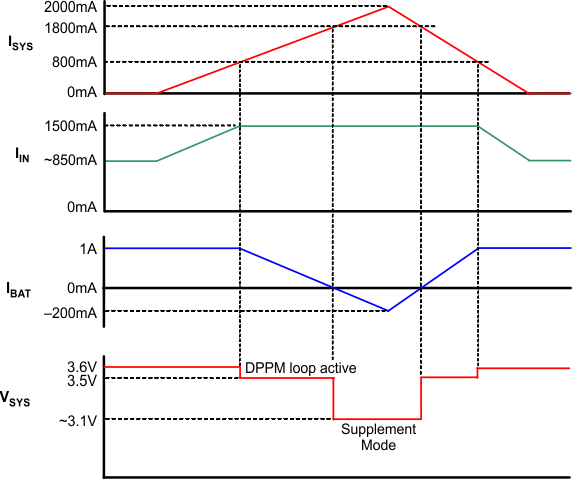 Figure 11. Example DPPM Response (VSupply = 5V, VBAT = 3.1V, 1.5A Input Current Limit)
7.4.9 Battery Discharge FET (BGATE)
The bq24266 contains a MOSFET driver to drive an external discharge FET between the battery and the system output. This external FET provides a low impedance path for supplying the system from the battery. Connect BGATE to the gate of the external discharge P-channel MOSFET. BGATE is on (low) under the following conditions:
- No input supply connected.
- IUSB1, IUSB2, IUSB3 pins = high
7.4.10 IUSB1, IUSB2, and IUSB3 Input
The bq24266 has three inputs that configure the input current limit and VINDPM thresholds. These input are also used to enable the USB OTG Boost function. The bq24266 incorporates all of the necessary input current limits to support USB2.0 and USB3.0 standards, as well as 1.5A to support wall adapters. Driving IUSB1, IUSB2, and IUSB3 all high places the bq24266 in Hi-Z mode where the buck converter is shutdown regardless if an input is connected to IN. Table 1 shows the configuration for IUSB1, IUSB2, and IUSB3.
Table 1. IUSB1, IUSB2, and IUSB3 Configurations
| IUSB3 | IUSB2 | IUSB1 | MODE | INPUT CURRENT LIMIT | VINDPM THRESHOLD |
|---|---|---|---|---|---|
| 0 | 0 | 0 | Charger | 100mA | 4.28V |
| 0 | 0 | 1 | Charger | 500mA | 4.44V |
| 0 | 1 | 0 | Charger | 1.5A | External |
| 0 | 1 | 1 | Boost | --- | --- |
| 1 | 0 | 0 | Charger | 150mA | 4.28V |
| 1 | 0 | 1 | Charger | 900mA | 4.44V |
| 1 | 1 | 0 | Charger | 2500mA | External |
| 1 | 1 | 1 | High Impedance | --- | --- |
7.4.11 Safety Timer in Charge Mode
At the beginning of the charging process, the bq24266 starts the safety timer. This timer is active during the entire charging process. If charging has not terminated before the safety timer expires, the IC enters suspend mode where charging is disabled. CE, or power must be toggled in order to clear the safety timer fault. The bq24266 also contains a 2X_TIMER that doubles the safety timer to prevent premature safety timer expiration when the charge current is reduced by a load on SYS or a NTC condition. When 2X_TIMER is active, the timer runs at half speed when any loop is active other than CC or CV. This includes VINDPM, input current limit, or thermal regulation. The timer also runs at half speed during TS warm/cool conditions.
7.4.12 LDO Output (DRV)
The bq24266 contains a linear regulator (DRV) that is used to supply the internal MOSFET drivers and other circuitry. Additionally, DRV supplies up to 10mA external loads to power the PG or CHG LED or the USB transceiver circuitry. The maximum value of the DRV output is 5.3V so it ideal to protect voltage sensitive USB circuits. The LDO is on whenever a supply is connected to the input of the bq24266. The DRV is disabled under the following conditions:
- VSUPPLY < UVLO
- VSUPPLY < VBAT + VSLP
- Thermal Shutdown
7.4.13 External NTC Monitoring (TS)
The bq24266 provides a flexible, voltage based TS input for monitoring the battery pack NTC thermistor. The bq24266 implements the full JEITA standard. The voltage at TS is monitored to determine that the battery is at a safe temperature during charging. The JEITA specification is shown in Figure 12.
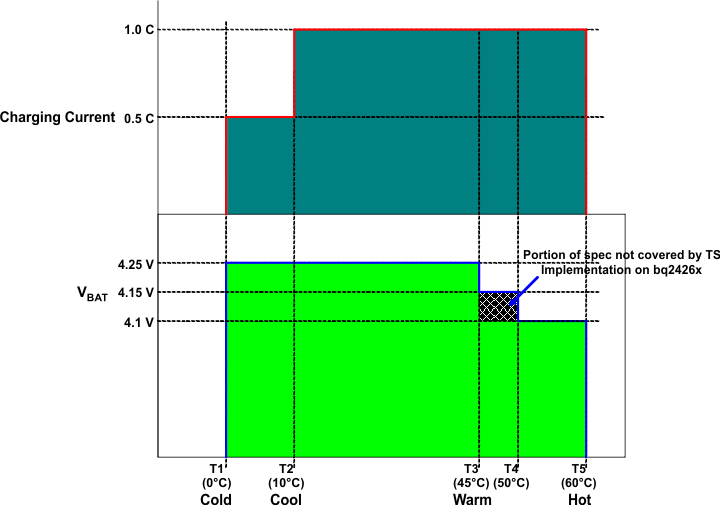 Figure 12. Charge Current During TS Conditions
To satisfy the JEITA requirements, four temperature thresholds are monitored; the cold battery threshold (TNTC < 0°C), the cool battery threshold (0°C < TNTC < 10°C), the warm battery threshold (45°C < TNTC < 60°C) and the hot battery threshold (TNTC > 60°C). These temperatures correspond to the VCOLD, VCOOL, VWARM, and VHOT thresholds in the EC table. Charging is suspended and timers are suspended when VTS < VHOT or VTS > VCOLD. When VCOOL < VTS < VCOLD, the charging current is reduced to half of the programmed charge current. When VHOT < VTS < VWARM, the battery regulation voltage is reduced to 4.06V from the 4.2V regulation threshold. The TS function is disabled by connecting TS directly to DRV (VTS > VTSOFF).
The TS function is voltage based for maximum flexibility. Connect a resistor divider from DRV to GND with TS connected to the center tap to set the threshold. The connections are shown in Figure 13. The resistor values are calculated using the following equations:


Where:
VCOLD = 0.60 × VDRV
VHOT = 0.30 × VDRV


Where RHOT is the NTC resistance at the hot temperature and RCOLD is the NTC resistance at cold temperature.
The WARM and COOL thresholds are not independently programmable. The COOL and WARM NTC resistances for a selected resistor divider are calculated using Equation 5 and Equation 6.
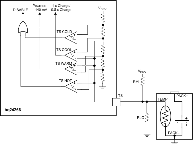 Figure 13. TS Circuit
7.4.14 Thermal Regulation and Protection
During the charging process, to prevent overheating in the chip, bq24266 monitors the junction temperature, TJ, of the die and reduces the input current once TJ reaches the thermal regulation threshold, TREG. The input current is reduced to zero when the junction temperature increases about 10°C above TREG. Once the input current is reduced to 0, the system current is reduced while the battery supplements the load to supply the system. When the input current is completely reduced to 0 and TJ>125°C, this is may cause a thermal shutdown of the bq24266 if the die temperature rises too high. At any state, if TJ exceeds TSHTDWN, bq24266 stops charging and disables the buck converter. During thermal shutdown mode, PWM is turned off and all timers are suspended. The charge cycle resumes when TJ falls below TSHTDWN by approximately 10°C.
7.4.15 Status Outputs (CHG, PG)
The CHG and PG outputs are used to indicate operating conditions for the bq24266. The PG output indicates that a valid input source is connected to VIN. PG is low when (VBAT + VSLP) < VIN < VOVP. When there is no supply connected to the input within this range, PG is high impedance. Table 2 illustates the PG behavior under different conditions.
Table 2. PG Behavior
| CHARGE STATE | PG BEHAVIOR |
|---|---|
| VSUPPLY < VUVLO | High Impedance |
| VSUPPLY < (VBAT + VSLP) | High Impedance |
| (VBAT + VSLP) < VIN < VOVP | Low |
| VSUPPLY > VOVP | High Impedance |
The CHG output indicates new charge cycles. When a new charge cycle is initiated by CE or toggling the input power, CHG goes low and remains low until termination. After termination, CHG remains high impedance until a new charge cycle is initiated or the battery is removed/re-inserted. CHG does not go low during recharge cycles. Table 3 illustrates the CHG behavior under different conditions.
Connect PG and CHG to the DRV output through an LED for visual indication, or connect through a 100kΩ pullup to the required logic rail for host indication.
Table 3. CHG Behavior
| CHARGE STATE | CHG BEHAVIOR |
|---|---|
| Charge in Progress | Low (first charge cycle) High-Impedance (recharge cycles) |
| Charge suspended by /CE or TS function | |
| Charging Suspended by Thermal Loop | |
| Charging Done | High-Impedance |
| Recharge Cycle after Termination | |
| Timer Fault | |
| No Valid Supply VIN > VOVP or VIN < (VBAT + VSLP) |
|
| No Battery Present |
7.4.16 Boost Mode Operation
When the IUSB inputs are configured in Boost Mode (IUSB3 = 0, IUSB2 = IUSB1 = 1), the device operates in boost mode and delivers 5V to IN to supply USB OTG devices connected to the USB connector.
7.4.16.1 PWM Controller in Boost Mode
Similar to charge mode operation, in boost mode the IC switches at 1.5MHz to regulate the voltage at IN to 5V. The voltage control loop is internally compensated to provide enough phase margin for stable operation with the the battery from 3.3V to 4.2V up to 1A.
In boost mode, the cycle-by-cycle current limit is set to 4A to provide protection against short circuit conditions. If the cycle-by-cycle current limit is active for 8ms, an overload condition is detected and the device exits boost mode, and signals an over-current fault. Additionally, discharge current limit (ILIM(DISCHG)) is active to protect the battery from overload. Synchronous operation and burst mode are used to maximize efficiency over the full load range.
The bq24266 will not enter boost mode unless the IN voltage is less than the UVLO. When the boost function is enabled, the bq24266 enters a linear mode to bring IN up to the battery voltage. Once VIN > (VBAT – 1V), the bq24266 begins switching and regulates IN up to 5V. If VIN does not rise to within 1V of VBAT within 8ms, an over-current event is detected and boost mode is exited.
7.4.16.2 Burst Mode during Light Load
In boost mode, the IC operates using burst mode to improve light load efficiency and reduce power loss. During boost mode, the PWM converter is turned off when the device reaches minimum duty cycle and the output voltage rises to VBURST(ENT) threshold. This corresponds to approximately a 75mA inductor current. The converter then restarts when VIN falls to VBURST(EXT). See Figure 22 in the Typical Operating Characteristics for an example waveform.
7.4.16.3 CHG and PG During Boost Mode
During boost mode, the CHG and PG outputs are high impedance.
7.4.16.4 Protection in Boost Mode
7.4.16.4.1 Output Over-Voltage Protection
The bq24266 contains integrated over-voltage protection on the IN pin. During boost mode, if an over-voltage condition is detected (VIN > VBOOSTOVP), after deglitch tDGL(BOOST_OVP), the IC turns off the PWM converter unitl the IUSB pins are toggled. The converter does not restart when VIN drops to the normal level until the IUSB pins are toggled.
7.4.16.4.2 Output Over-Current Protection
The bq24266 contains over current protection to prevent the device and battery damage when IN is overloaded. When an over-current condition occurs, the cycle-by-cycle current limit limits the current from the battery to the load. If the overload condition lasts for 8ms, the overload fault is detected. When an overload condition is detected, the bq24266 turns off the PWM converter. The boost operation starts only after the fault is cleared and the IUSB pins are toggled.
7.4.16.4.3 Battery Voltage Protection
During boost mode, when the battery voltage is below the minimum battery voltage threshold, VBATUVLO, the IC turns off the PWM converter. Once the battery voltage returns to the acceptable level, the boost starts only after the IUSB pins are toggled. Proper operation below 3.3V down to the VBATUVLOis not specified.
