SLUSBY7 July 2014
PRODUCTION DATA.
- 1 Features
- 2 Applications
- 3 Description
- 4 Revision History
- 5 Description (Continued)
- 6 Pin Configuration and Functions
- 7 Specifications
-
8 Detailed Description
- 8.1 Overview
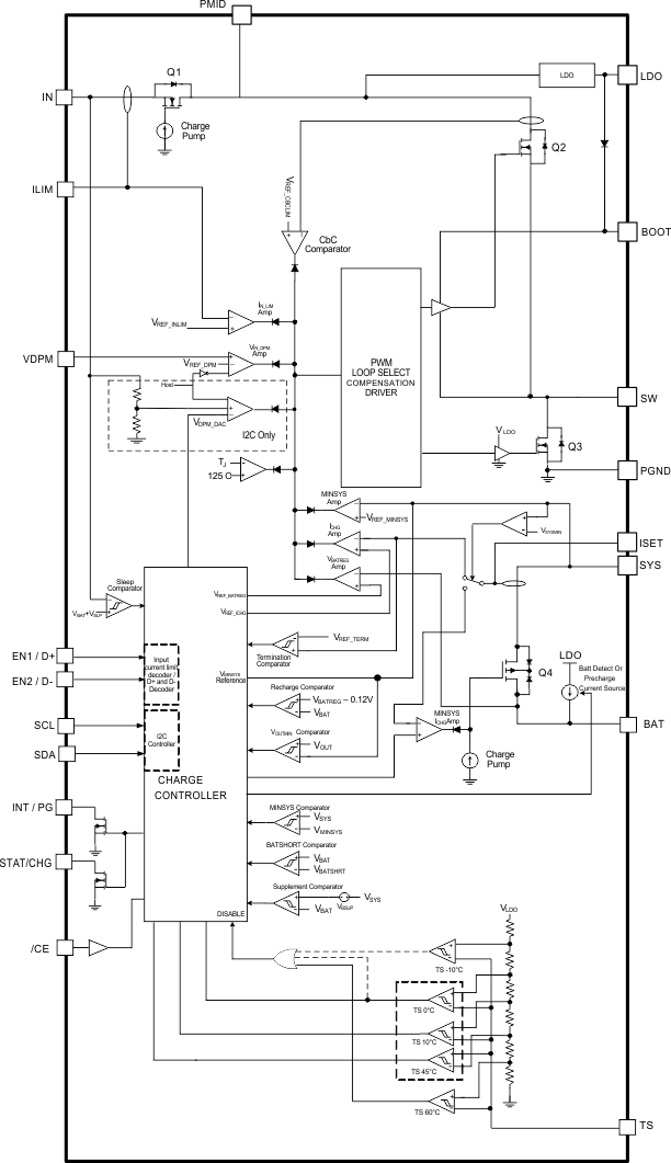
- 8.2 Functional Block Diagram
- 8.3 Feature Description
- 8.4
Device Functional Modes
- 8.4.1 Charge Profile
- 8.4.2 EN1/EN2 Pins
- 8.4.3 I2C Operation (Host Mode / Default Mode)
- 8.4.4 External Settings: ISET, ILIM and VIN_DPM
- 8.4.5 Transient Response
- 8.4.6 Input Voltage Based DPM
- 8.4.7 Sleep Mode
- 8.4.8 Input Over-Voltage Protection
- 8.4.9 NTC Monitor
- 8.4.10 Safety Timer
- 8.4.11 Watchdog Timer
- 8.4.12 Thermal Regulation and Thermal Shutdown
- 8.4.13 Fault Modes
- 8.4.14 Serial Interface Description
- 8.5 Register Maps
- 9 Application and Implementation
- 10Power Supply Recommendations
- 11Layout
- 12Device and Documentation Support
- 13Mechanical, Packaging, and Orderable Information
8 Detailed Description
8.1 Overview
The bq24250C is a highly-integrated, single-cell, Li-Ion battery charger with integrated current sense resistors targeted for space-limited, portable applications with high-capacity batteries. The single-cell charger has a single input that operates from either a USB port or AC wall adapter for a versatile solution.
The bq24250C device has two modes of operation: 1) I2C mode, and 2) standalone mode. In I2C mode, the host adjusts the charge parameters and monitors the status of the charger operation. In standalone mode, the external resistor sets the input-current limit, and charge current limit. Standalone mode also serves as the default settings when a DCP adapter is present. It enters host mode while the I2C registers are accessed and the watchdog timer has not expired (if enabled). The battery is charged in four phases: trickle charge, pre-charge, constant current and constant voltage. In all charge phases, an internal control loop monitors the IC junction temperature and reduces the charge current if the internal temperature threshold is exceeded.
8.2 Functional Block Diagram
8.3 Feature Description
8.3.1 Dynamic Power Path Management
The bq24250C features a SYS output that powers the external system load connected to the battery. This output is active whenever a valid source is connected to IN or BAT. The following discusses the behavior of SYS with a source connected to the supply or a battery source only.
When a valid input source is connected to the input and the charge is enabled, the charge cycle is initiated. In case of VBAT > ~3.5V, the SYS output is connected to VBAT. If the SYS voltage falls to VMINSYS, it is regulated to the VSYSREG threshold to maintain the system output even with a deeply discharged or absent battery. In this mode, the SYS output voltage is regulated by the buck converter and the battery FET is linearly regulated to regulate the charge current into the battery. The current from the supply is shared between charging the battery and powering the system load at SYS.
The dynamic power path management (DPPM) circuitry of the bq24250C monitors the current limits continuously and if the SYS voltage falls to the VMINSYS voltage, it adjusts charge current to maintain the minimum system voltage and supply the load on SYS. If the charge current is reduced to zero and the load increases further, the bq24250C enters battery supplement mode. During supplement mode, the battery FET is turned on and the battery supplements the system load.
If the battery is ever 5% above the regulation threshold, the battery OVP circuit shuts the PWM converter off and the battery FET is turned on to discharge the battery to safe operating levels. Battery OVP FAULT is shown in the I2C FAULT registers.
When no input source is available at the input and the battery is connected, the battery FET is turned on similar to supplement mode. The battery must be above VBATUVLO threshold to turn on the SYS output. In this mode, the current is not regulated;
8.3.2 Production Test Mode
To aid in end mobile device product manufacturing, the bq24250C includes a Production Test Mode (PTM), where the device is essentially a DC-DC buck converter. In this mode the input current limit to the charger is disabled and the output current limit is limited only by the inductor cycle-by-cycle current (e.g. 3.5A). The PTM mode can be used to test systems with high transient loads such as GSM transmission without the need of a battery being present.
As a means of safety, the Anyboot algorithm determines if a battery is not present at the output prior to enabling the PTM mode. If a battery is present and the software attempts to enter PTM mode, the device will not enable PTM mode.
8.3.3 AnyBoot Battery Detection
The bq24250C includes a sophisticated battery detection algorithm used to provide the system with the proper status of the battery connection. The AnyBoot battery algorithm also ensures the detection of voltage based battery protectors that may have a long closure time (due to the hysteresis of the protection switch and the cell capacity). The AnyBoot battery detection algorithm utilizes a dual-voltage based detection methodology where the system rail switches between two primary voltage levels. The period of the voltage level shift is 64ms and therefore the power supply rejection of the down-system electronics detects this shift as essentially DC.
The AnyBoot algorithm has essentially 3 states. The 1st state is used to determine if the device has terminated with a battery attached. If it has terminated due to the battery not being present, then the algorithm moves to the 2nd and 3rd states. The 2nd and 3rd states shift the system voltage level between 4.2V and 3.72V. In each state there are comparator checks to determine if a battery has been inserted. The two states ensure the detection of a battery even if the voltage of the cell is at the same level of the comparator thresholds. The algorithm will remain in states 2 and 3 until a battery has been inserted. The flow diagram details for the Anyboot algorithm are shown in Figure 14.
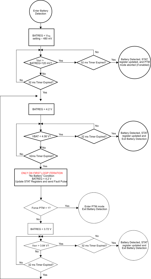 Figure 14. AnyBoot Battery Detection Flow Diagram
8.4 Device Functional Modes
8.4.1 Charge Profile
The bq24250C provides a switch-mode buck regulator with output power path and a charge controller to provide optimum performance over the full battery charge cycle. The control loop for the buck regulator has 7 primary feedback loops that can set the duty cycle:
- Constant Current (CC)
- Constant Voltage (CV)
- Minimum System Voltage (MINSYS)
- Input Current (IILIM)
- Input Voltage (VIN_DPM)
- Die Temperature
- Cycle by Cycle Current
The feedback with the minimum duty cycle will be chosen as the active loop. The bq24250C supports a precision Li-Ion or Li-Polymer charging system for single-cell applications. The Dynamic Power Path Management (DPPM) feature regulates the system voltage to a minimum of VMINSYS, so that startup is enabled even with a missing or deeply discharged battery. This provides a much better overall user experience in mobile applications. The figure below illustrates a typical charge profile while also demonstrating the minimum system output voltage regulation.
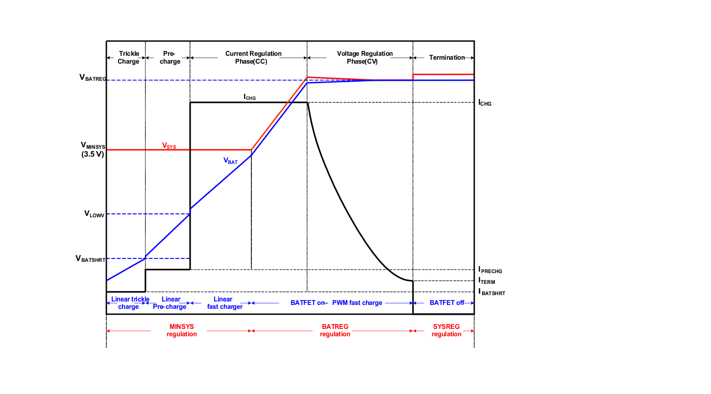 Figure 15. Typical Charge Profile
Figure 16 demonstrates a measured charge profile with the bq24250C while charging a 2700mAh Li-Ion battery at a charge rate of 1A.
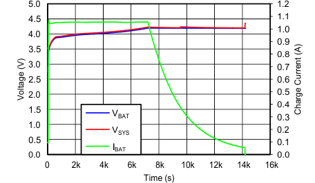 Figure 16. bq24250C Charge Profile while Charging a 2700 mAh Battery at a 1A Charge Rate
Figure 17 illustrates the precharge behavior of the above charge profile by narrowing the time axis to 0 – 120 seconds.
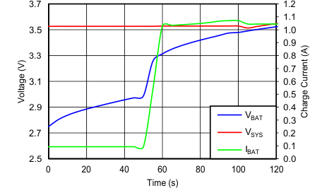 Figure 17. bq24250C Charge Profile While Charging a 2700-mAh Battery at a 1A Charge During Precharge
8.4.2 EN1/EN2 Pins
The bq24250C is I2C and Stand Alone part. The EN1 and EN2 pins are available in this IC spin to support USB 2.0 compliance. These pins are used for Input Current Limit Configuration I. Set EN1 and EN2 to control the maximum input current and enable USB compliance. See Table 1 below for programming details.
When the input current limit pins change state, the VIN_DPM threshold changes as well. See Table 1 for the detailed truth table:
Table 1. EN1, and EN2 Truth Table(1)
| EN2 | EN1 | Input Current Limit | VIN_DPM Threshold |
|---|---|---|---|
| 0 | 0 | 500mA | 4.36V |
| 0 | 1 | Externally programmed by ILIM (up to 2.0A) | Externally programmed VDPM |
| 1 | 0 | 100mA | 4.36V |
| 1 | 1 | Input Hi-Z | None |
8.4.3 I2C Operation (Host Mode / Default Mode)
There are two primary modes of operation when interacting with the charge parameters of the bq24250C charger: 1) Host mode operation where the I2C registers set the charge parameters, and 2) Default mode where the register defaults set the charge parameters.
Figure 18 illustrates the behavior of the bq24250C when transitioning between host mode and stand alone mode:
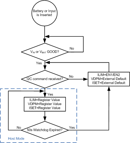 Figure 18. Host Mode and Stand Alone Mode Handoff
Once the battery or input is inserted and above the good thresholds, the device determines if an I2C command has been received in order to discern whether to operate from the I2C registers or the internal register defaults. In stand-alone mode the input current limit is set by the EN1/EN2 pins. If the watch dog timer is enabled, the device will enter stand alone operation once the watchdog timer expires and re-initiate the default charge settings.
8.4.4 External Settings: ISET, ILIM and VIN_DPM
If the external resistor settings are used, the following equations can be followed to configure the charge settings.
The fast charge current resistor (RISET) can be set by using the following formula:
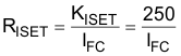
Where IFC is the desired fast charge current setting in Amperes.
The input current limit resistor (RILIM) can be set by using the following formula:
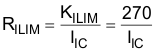
Where IIC is the desired input current limit in Amperes.
Based on the application diagram reference designators, the resistor R1 and R2 can be calculated as follows to set VIN_DPM:
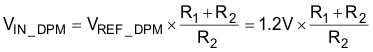
VIN_DPM should be chosen first along with R1. Choosing R1 first will ensure that R2 will be greater than the resistance chosen. This is the case since VIN_DPM should be chosen to be greater than 2x VREF_DPM.
If external resistors are not desired in order to reduce the BOM count, the VDPM and the ILIM pins can be shorted to set the internal defaults. The ISET resistor cannot be shorted in order to avoid an unstable charging state.Note that floating the ILIM pin will result in zero charge current if the external ISET is configured via the I2C register. Table 2 summarizes the settings when the ILIM, ISET, and VIN_DPM pins are shorted to GND:
Table 2. ILIM, VDPM, and ISET Short Behaviors
| PIN SHORTED | BEHAVIOR |
|---|---|
| ILIM | Input current limit = 2A |
| VDPM | VIN_DPM = 4.68V |
| ISET | Fault—Charging Suspended |
8.4.5 Transient Response
The bq24250C includes an advanced hybrid switch mode control architecture. When the device is regulating the charge current (fast-charge), a traditional voltage mode control loop is used with a Type-3 compensation network. However, the bq24250C switches to a current mode control loop when the device enters voltage regulation. Voltage regulation occurs in three charging conditions: 1) Minimum system voltage regulation (battery below MINSYS), 2) Battery voltage regulation (IBAT < ICHG), and 3) Charge Done (VSYS = VBAT + 3.5%). This architecture allows for superior transient performance when regulating the voltage due to the simplification of the compensation when using current mode control. The below transient response plot illustrates a 0A to 2A load step with 4.7ms full cycle and 12% duty cycle. A 3.9V Li-Ion battery is used. The input voltage is set to 5V, charge current is set to 0.5A and the input current is limited to 0.5A. Note that a high line impedance input supply was used to indicate a realistic input scenario (adapter and cable). This is illustrated by the change in VIN seen at the input of the IC.
Figure 19 shows a ringing at both the input voltage and the input current. This is caused by the input current limit speed up comparator.
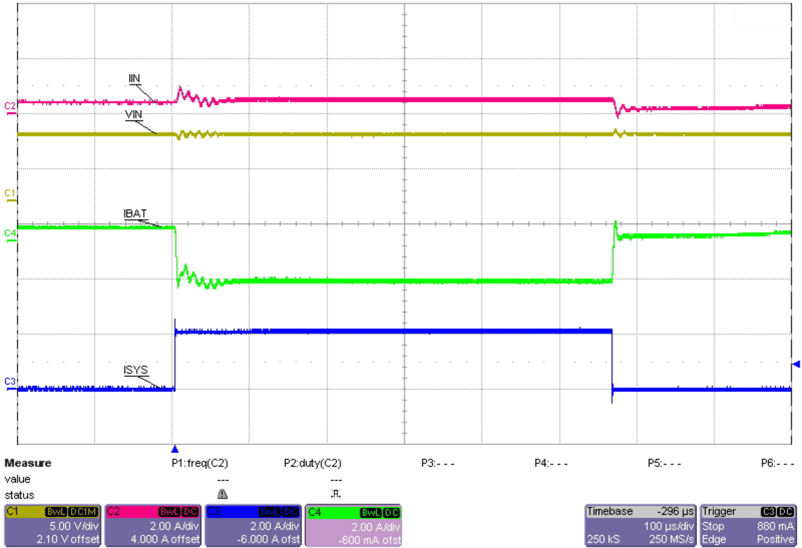 Figure 19. 2A Load Step Transient
8.4.6 Input Voltage Based DPM
During normal charging process, if the input power source is not able to support the programmed or default charging current, the supply voltage deceases. Once the supply drops to VIN_DPM, the input current limit is reduced down to prevent the further drop of the supply. When the IC enters this mode, the charge current is lower than the set. This feature ensures IC compatibility with adapters with different current capabilities without a hardware change.
8.4.7 Sleep Mode
The bq24250C enters the low-power sleep mode if the voltage on VIN falls below sleep-mode entry threshold, VBAT+VSLP, and VIN is higher than the under-voltage lockout threshold, VUVLO. This feature prevents draining the battery during the absence of VIN. When VIN < VBAT+VSLP, the bq24250C turns off the PWM converter, turns on the battery FET, sends a single 256µs pulse is sent on the STAT and INT outputs and the FAULT/STAT bits of the status registers are updated in the I2C. Once VIN > VBAT+VSLP with the hysteresis, the FAULT bits are cleared and the device initiates a new charge cycle.
8.4.8 Input Over-Voltage Protection
The bq24250C provides over-voltage protection on the input that protects downstream circuitry. The built-in input over-voltage protection to protect the device and other components against damage from overvoltage on the input supply (Voltage from VIN to PGND). When VIN > VOVP, the bq24250C turns off the PWM converter, turns the battery FET, sends a single 256μs pulse is sent on the STAT and INT outputs and the FAULT/STAT bits of the status registers and the battery/supply status registers are updated in the I2C. Once the OVP fault is removed, the FAULT bits are cleared and the device returns to normal operation. The OVP threshold for the bq24250 is programmable from 6.5V to 10.5V using VOVP bits in register #7.
8.4.9 NTC Monitor
The bq24250C includes the integration of an NTC monitor pin that complies with a modified JEITA specification (PSE also available upon request). The voltage based NTC monitor allows for the use of any NTC resistor with the use of the circuit shown in Figure 20.
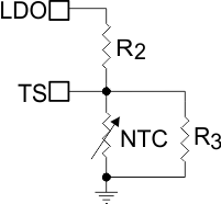 Figure 20. Voltage Based NTC circuit
The use of R3 is only necessary when the NTC does not have a beta near 3500K. When deviating from this beta, error will be introduced in the actual temperature trip thresholds. The trip thresholds are summarized below which are typical values provided in the specification table. Note that the TWARM threshold is just a warning for the warm temperature, the device will generate an interrupt but it will not affect the charging process.
Table 3. Ratiometric TS Trip Thresholds
| VHOT | 30.0% |
| VWARM | 38.3% |
| VCOOL | 48.5% |
| VCOLD | 60% |
When sizing for R2 and R3, it is best to solve two simultaneous equations that ensure the temperature profile of the NTC network will cross the VHOT and VCOLD thresholds. The accuracy of the VWARM and VCOOL threshold will depend on the beta of the chosen NTC resistor. The two simultaneous equations are shown below:
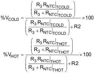
Where the NTC resistance at the VHOT and VCOLD temperatures must be resolved as follows:
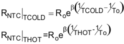
To be JEITA compliant, TCOLD must be 0°C and THOT must be 60°C. If an NTC resistor is chosen such that the beta is 4000K and the nominal resistance is 10kΩ, the following R2 and R3 values result from the above equations:
R2 = 5 kΩ
R3 = 9.82 kΩ
Figure 21 illustrates the temperature profile of the NTC network with R2 and R3 set to the above values.
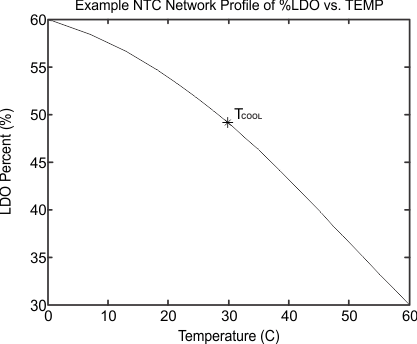 Figure 21. Voltage Based NTC Circuit Temperature Profile
Once the resistors are configured, the internal JEITA algorithm will apply the below profile at each trip point for battery voltage regulation and charge current regulation.
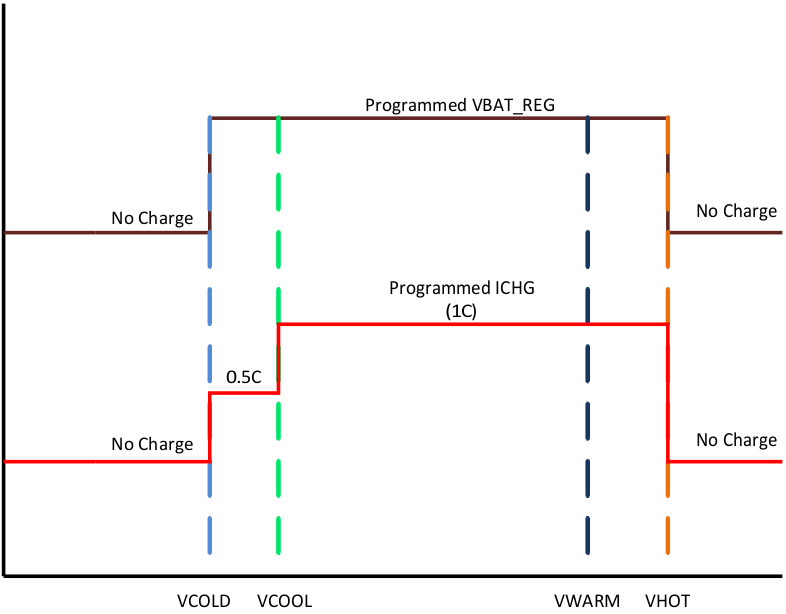 Figure 22. Modified JEITA Profile for Voltage and Current Regulation Loops
8.4.10 Safety Timer
At the beginning of charging process, the bq24250C starts the safety timer. This timer is active during the entire charging process. If charging has not terminated before the safety timer expires, the IC enters suspend mode where charging is disabled. The safety timer time is selectable using the I2C interface. A single 256μs pulse is sent on the STAT and INT outputs and the FAULT/ bits of the status registers are updated in the I2C. This function prevents continuous charging of a defective battery if the host fails to reset the safety timer. When 2xTMR_EN bit is set to “1”, the safety timer runs at a rate 2x slower than normal (the timer is extended) under the following conditions:
- Pre-charge or linear mode (minimum system voltage mode),
- During thermal regulation where the charge current is reduced,
- During TS fault where the charge current is reduced
The safety timer is suspended during OVP, TS fault where charge is disabled, thermal shut down, and sleep mode.
8.4.11 Watchdog Timer
In addition to the safety timer, the bq24250C contains a 50-second watchdog timer that monitors the host through the I2C interface. Once a write is performed on the I2C interface, a watchdog timer is reset and started. The watchdog timer can be disabled by writing “0” on WD_EN bit of register #1. Writing “1” on that bit enables it and reset the timer.
If the watchdog timer expires, the IC enters DEFAULT mode where the default charge parameters are loaded and charging continues. The I2C may be accessed again to re-initialize the desired values and restart the watchdog timer as long as the safety timer has not expired. Once the safety timer expires, charging is disabled.
8.4.12 Thermal Regulation and Thermal Shutdown
During the charging process, to prevent overheat of the chip, bq24250C monitors the junction temperature, TJ, of the die and begins to taper down the charge current once TJ reaches the thermal regulation threshold, TREG. The charge current is reduced when the junction temperature increases above TREG. Once the charge current is reduced, the system current is reduced while the battery supplements the load to supply the system. This may cause a thermal shutdown of the IC if the die temperature rises too. At any state, if TJ exceeds TSHTDWN, bq24250C suspends charging and disables the buck converter. During thermal shutdown mode, PWM is turned off, all safety timers are suspended, and a single 256μs pulse is sent on the STAT and INT outputs and the FAULT/STAT bits of the status registers are updated in the I2C. A new charging cycle begins when TJ falls below TSHTDWN by approximately 10°C.
8.4.13 Fault Modes
The bq24250C includes several hardware fault detections. This allows for specific conditions that could cause a safety concern to be detected. With this feature, the host can be alleviated from monitoring unsafe charging conditions and also allows for a “fail-safe” if the host is not present. The table below summarizes the faults that are detected and the resulting behavior.
| FAULT CONDITION | CHARGER BEHAVIOR | SAFETY TIMER BEHAVIOR |
|---|---|---|
| Input OVP | VSYS and ICHG Disabled | Suspended |
| Input UVLO | VSYS and ICHG Disabled | Reset |
| Sleep (VIN < VBAT) | VSYS and ICHG Disabled | Suspended |
| TS Fault (Batter Over Temp) | VSYS Active and ICHG Disabled | Suspended |
| Thermal Shutdown | VSYS and ICHG Disabled | Suspended |
| Timer Fault | VSYS Active and ICHG Disabled | Reset |
| No Battery | VSYS Active and ICHG Disabled | Suspended |
| ISET Short | VSYS Active and ICHG Disabled | Suspended |
| Input Fault & LDO Low | VSYS and ICHG Disabled | Suspended |
8.4.14 Serial Interface Description
The bq24250C uses an I2C compatible interface to program charge parameters. I2C is a 2-wire serial interface developed by NXP (formerly Philips Semiconductor, see I2C-Bus Specification, Version 5, October 2012). The bus consists of a data line (SDA) and a clock line (SCL) with pull-up structures. When the bus is idle, both SDA and SCL lines are pulled high. All the I2C compatible devices connect to the I2C bus through open drain I/O pins, SDA and SCL. A master device, usually a microcontroller or a digital signal processor, controls the bus. The master is responsible for generating the SCL signal and device addresses. The master also generates specific conditions that indicate the START and STOP of data transfer. A slave device receives and/or transmits data on the bus under control of the master device.
Thebq24250C device works as a slave and supports the following data transfer modes, as defined in the I2C Bus™ Specification: standard mode (100 kbps) and fast mode (400 kbps). The interface adds flexibility to the battery charge solution, enabling most functions to be programmed to new values depending on the instantaneous application requirements. The I2C circuitry is powered from IN when a supply is connected.
The data transfer protocol for standard and fast modes is exactly the same; therefore, they are referred to as the F/S-mode in this document. The bq24250C device only supports 7-bit addressing. The device 7-bit address is defined as ‘1101010’ (0x6Ah).
To avoid I2C hang-ups, a timer (tI2CRESET) runs during I2C transactions. If the transaction takes longer than tI2CRESET, any additional commands are ignored and the I2C engine is reset. The timeout is reset with START and repeated START conditions and stops when a valid STOP condition is sent.
8.4.14.1 F/S Mode Protocol
The master initiates data transfer by generating a start condition. The start condition is when a high-to-low transition occurs on the SDA line while SCL is high, as shown in Figure 23. All I2C -compatible devices should recognize a start condition.
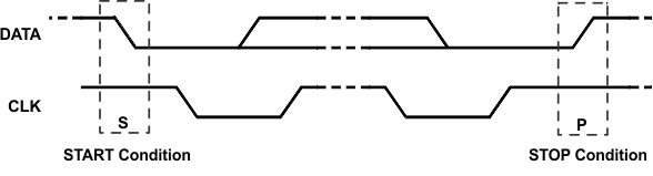 Figure 23. START and STOP Condition
The master then generates the SCL pulses, and transmits the 7-bit address and the read/write direction bit R/W on the SDA line. During all transmissions, the master ensures that data is valid. A valid data condition requires the SDA line to be stable during the entire high period of the clock pulse (see Figure 24). All devices recognize the address sent by the master and compare it to their internal fixed addresses. Only the slave device with a matching address generates an acknowledge (see Figure 25) by pulling the SDA line low during the entire high period of the ninth SCL cycle. Upon detecting this acknowledge, the master knows that communication link with a slave has been established.
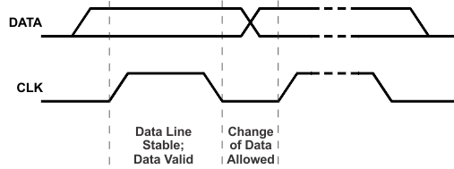 Figure 24. Bit Transfer on the Serial Interface
The master generates further SCL cycles to either transmit data to the slave (R/W bit 0) or receive data from the slave (R/W bit 1). In either case, the receiver needs to acknowledge the data sent by the transmitter. So an acknowledge signal can either be generated by the master or by the slave, depending on which one is the receiver. The 9-bit valid data sequences consisting of 8-bit data and 1-bit acknowledge can continue as long as necessary. To signal the end of the data transfer, the master generates a stop condition by pulling the SDA line from low to high while the SCL line is high (see Figure 23). This releases the bus and stops the communication link with the addressed slave. All I2C compatible devices must recognize the stop condition. Upon the receipt of a stop condition, all devices know that the bus is released, and wait for a start condition followed by a matching address. If a transaction is terminated prematurely, the master needs to send a STOP condition to prevent the slave I2C logic from remaining in a incorrect state. Attempting to read data from register addresses not listed in this section will result in 0xFFh being read out.
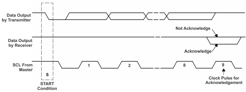 Figure 25. Acknowledge on the I2C Bus
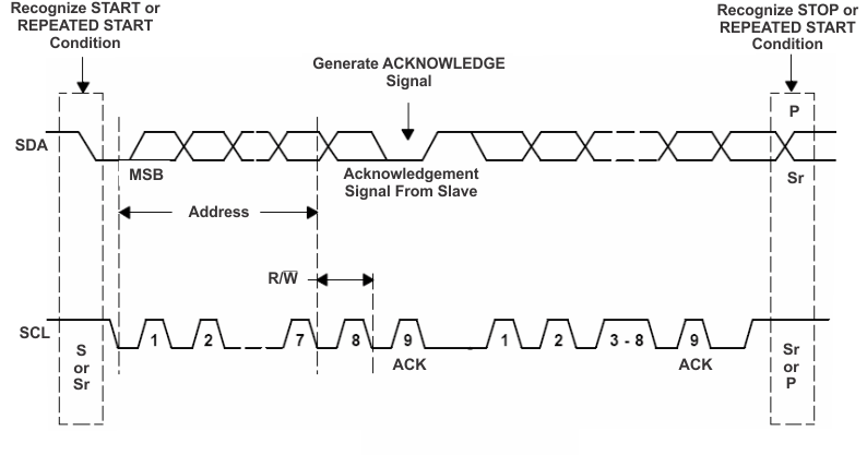 Figure 26. Bus Protocol
8.5 Register Maps
Register #1
Memory location: 00, Reset state: x0xx xxxx
| BIT | NAME | READ/WRITE | FUNCTION |
|---|---|---|---|
| B7(MSB) | WD_FAULT | Read only | Read:0 – No fault 1 – WD timeout if WD enabled |
| B6 | WD_EN | Read/Write | 0 – Disable 1 – Enable (also resets WC timer) |
| B5 | STAT_1 | Read only | 00 – Ready 01 – Charge in progress 10 – Charge done 11 – Fault |
| B4 | STAT_0 | Read only | |
| B3 | FAULT_3 | Read only | 0000 – Normal 0001 – Input OVP 0010 – Input UVLO 0011 – Sleep 0100 – Battery Temperature (TS) Fault 0101 – Battery OVP 0110 – Thermal Shutdown 0111 – Timer Fault 1000 – No Battery connected 1001 – ISET short 1010 – Input Fault and LDO low |
| B2 | FAULT_2 | Read only | |
| B1 | FAULT_1 | Read only | |
| B0(LSB) | FAULT_0 | Read only |
| WD_FAULT | ‘0’ indicates no watch dog fault has occurred, where a ‘1’ indicates a fault has previously occurred. | |
| WD_EN | Enables or disables the internal watch dog timer. A ‘1’ enables the watch dog timer and a ‘0’ disables it. '1' is default for bq24251 only. | |
| STAT | Indicates the charge controller status. | |
| FAULT | Indicates the faults that have occurred. If multiple faults occurred, they can be read by sequentially addressing this register (e.g. reading the register 2 or more times). Once all faults have been read and the device is in a non-fault state, the fault register will show “Normal”. Regarding the "Input Fault & LDO Low" the IC indicates this if LDO is low and at the same time the input is below UVLO or coming out of UVLO with LDO still low. | |
Register #2
Memory location: 01, Reset state: xxxx 1100
| BIT | NAME | READ/WRITE | FUNCTION |
|---|---|---|---|
| B7(MSB) | Reset | Write only | Write: 1 – Reset all registers to default values 0 – No effect |
| B6 | IIN_ILIMIT_2 | Read/Write | 000 – USB2.0 host with 100mA current limit 001 – USB3.0 host with 150mA current limit 010 – USB2.0 host with 500mA current limit 011 – USB3.0 host with 900mA current limit 100 – Charger with 1500mA current limit 101 – Charger with 2000mA current limit 110 – External ILIM current limit 111- No input current limit with internal clamp at 3A (PTM MODE) |
| B5 | IIN_ILIMIT_1 | Read/Write | |
| B4 | IIN_ILIMIT _0 | Read/Write | |
| B3 | EN_STAT | Read/Write | 0 – Disable STAT function 1 – Enable STAT function |
| B2 | EN_TERM | Read/Write | 0 – Disable charge termination 1 – Enable charge termination |
| B1 | CE | Read/Write | 0 – Charging is enabled 1 – Charging is disabled |
| B0 (LSB) | HZ_MODE | Read/Write | 0 – Not high impedance mode 1 – High impedance mode |
| IIN_LIMIT | Sets the input current limit level. When in host mode this register sets the regulation level. However, when in standalone mode (e.g. no I2C writes have occurred after power up or the WD timer has expired) the external resistor setting for IILIM sets the regulation level. | |
| EN_STAT | Enables and disables the STAT pin. When set to a ‘1’ the STAT pin is enabled and function normally. When set to a ‘0’ the STAT pin is disabled and the open drain FET is in HiZ mode. | |
| EN_TERM | Enables and disables the termination function in the charge controller. When set to a ‘1’ the termination function will be enabled. When set to a ‘0’ the termination function will be disabled. When termination is disabled, there are no indications of the charger terminating (i.e. STAT pin or STAT registers). | |
| CE | The charge enable bit which enables or disables the charge function. When set to a ‘0’, the charger operates normally. With a valid input, when set the bit to a ‘1’, the charger is disabled by turning off the BAT FET between SYS and BAT. The SYS pin continues to stay active via the switch mode controller. Without a valid input, When set the bit to a '1', the BAT FET will not be turned off. | |
| HZ_MODE | Sets the charger IC into low power standby mode. When set to a ‘1’, the switch mode controller is disabled but the BAT FET remains ON to keep the system powered. When set to a ‘0’, the charger operates normally. | |
Register #3
Memory location: 02, Reset state: 1000 1111
| BIT | NAME | READ/WRITE | FUNCTION |
|---|---|---|---|
| B7(MSB) | VBATREG_5(1) | Read/Write | Battery Regulation Voltage: 640mV (default 1) |
| B6 | VBATREG_4(1) | Read/Write | Battery Regulation Voltage: 320mV (default 0) |
| B5 | VBATREG_3(1) | Read/Write | Battery Regulation Voltage: 160mV (default 0) |
| B4 | VBATREG_2(1) | Read/Write | Battery Regulation Voltage: 80mV (default 0) |
| B3 | VBATREG_1(1) | Read/Write | Battery Regulation Voltage: 40mV (default 1) |
| B2 | VBATREG_0(1) | Read/Write | Battery Regulation Voltage: 20mV (default 1) |
| B1(4)(5) | USB_DET_1/EN1 | Read Only | Return USB detection result or pin EN1/EN0 status – 00 – DCP detected / EN1=0, EN0=0 01 – CDP detected / EN1=0, EN0=1 10 – SDP detected / EN1=1, EN0=0 11 – Apple/TT or non-standard adaptor detected / EN1=1, EN0=1 |
| B0(LSB) | USB_DET_0/EN0 | Read Only |
| VBATREG | Sets the battery regulation voltage | |
| USB_DET/EN | Provides status of the D+/D– detection-results for spins that include the D+/D– pins or the state of EN1/EN2 for spins that include the EN1/EN2 pins | |
Register #4
Memory location: 03, Reset state: 1111 1000
| BIT | NAME | READ/WRITE | FUNCTION |
|---|---|---|---|
| B7(MSB) | ICHG_4(1)(2) | Read/Write | Charge current 800mA – (default 1) |
| B6 | ICHG_3(1)(2) | Read/Write | Charge current: 400mA – (default 1) |
| B5 | ICHG_2(1)(2) | Read/Write | Charge current: 200mA – (default 1) |
| B4 | ICHG_1(1)(2) | Read/Write | Charge current: 100mA – (default 1) |
| B3 | ICHG_0(1)(2) | Read/Write | Charge current: 50mA – (default 1) |
| B2 | ITERM_2(3) | Read/Write | Termination current sense threshold: 100mA (default 0) |
| B1 | ITERM_1(3) | Read/Write | Termination current sense threshold: 50mA (default 0) |
| B0(LSB) | ITERM_0(3) | Read/Write | Termination current sense threshold: 25mA (default 0) |
| ICHG | Sets the charge current regulation | |
| ITERM | Sets the current level at which the charger will terminate | |
Register #5
Memory location: 04, Reset state: xx00 x010
| BIT | NAME | READ/WRITE | FUNCTION |
|---|---|---|---|
| B7(MSB) | LOOP_STATUS1(1) | Read Only | 00 – No loop is active that slows down timer 01 – VIN_DPM regulation loop is active 10 – Input current limit loop is active 11 – Thermal regulation loop is active |
| B6 | LOOP_STATUS0(1) | Read Only | |
| B5 | LOW_CHG | Read/Write | 0 – Normal charge current set by 03h 1 – Low charge current setting 330mA (default 0) |
| B4 | DPDM_EN | Read/Write | 0 – Bit returns to 0 after D+/D– detection is performed 1 – Force D+/D– detection (default 0) |
| B3 | CE_STATUS | Read Only | 0 – CE low 1 – CE high |
| B2 | VINDPM_2(2) | Read/Write | Input VIN-DPM voltage: 320mV (default 0) |
| B1 | VINDPM_1(2) | Read/Write | Input VIN-DPM voltage: 160mV (default 1) |
| B0(LSB) | VINDPM_0(2) | Read/Write | Input VIN-DPM voltage: 80mV (default 0) |
| LOOP_STATUS | Provides the status of the active regulation loop. The charge controller allows for only one loop can regulate at a time. | |
| LOW_CHG | When set to a ‘1’, the charge current is reduced 330mA independent of the charge current setting in register 0x03. When set to ‘0’, the charge current is set by register 0x03. | |
| DPDM_EN | Forces a D+/D- detection routine to be executed once a ‘1’ is written. This is independent of the input being supplied. | |
| CE_STATUS | Provides the status of the CE pin level. If the CE pin is forced high, this bit returns a ‘1’. If the CE pin is forced low, this bit returns a ‘0’. | |
| VINDPM | Sets the input VDPM level. | |
Register #6
Memory location: 05, Reset state: 101x 1xxx
| BIT | NAME | READ/WRITE | FUNCTION |
|---|---|---|---|
| B7(MSB) | 2XTMR_EN | Read/Write | 0 – Timer not slowed at any time 1 – Timer slowed by 2x when in thermal regulation, VIN_DPM or DPPM (default 1) |
| B6 | TMR_1 | Read/Write | Safety Timer Time Limit 00 – 0.75 hour fast charge 01 – 6 hour fast charge (default 01) 10 – 9 hour fast charge 11 – Disable safety timers |
| B5 | TMR_2 | Read/Write | |
| B4 | SYSOFF | Read/Write | 0 – SYSOFF disabled 1 – SYSOFF enabled |
| B3 | TS_EN | Read/Write | 0 – TS function disabled 1 – TS function enabled (default 1) |
| B2 | TS_STAT2 | Read only | TS Fault Mode: 000 – Normal, No TS fault 100 – TS temp < TCOLD (Charging suspended for JEITA and Standard TS) 101 – TFREEZE < TS temp < TCOLD (Charging at 3.9V and 100mA and only for PSE option only) 110 – TS temp < TFREEZE (Charging suspended for PSE option only) 111 – TS open (TS disabled) |
| B1 | TS_STAT1 | Read only | |
| B0(LSB) | TS_STAT0 | Read only |
| 2xTMR_EN | When set to a ‘1’, the 2x Timer function is enabled and allows for the timer to be extended if a condition occurs where the charge current is reduced (i.e. VIN_DPM, thermal regulation, etc.). When set to a ‘0’, this function is disabled and the normal timer will always be executed independent of the current reduce conditions. | |
| SYSOFF | When set to a ‘1’ and the input is removed, the internal battery FET is turned off in order to reduce the leakage from the BAT pin to less than 1µA. Note that this disconnects the battery from the system. When set to a ‘0’, this function is disabled. | |
| TS_EN | Enables and disables the TS function. When set to a ‘0’ the TS function is disabled otherwise it is enabled. Only applies to spins that have a TS pin. | |
| TS_STAT | Provides status of the TS pin state for spins that have a TS pin. | |
Register #7
Memory location: 06, Reset state: 1110 0000
| BIT | NAME | READ/WRITE | FUNCTION |
|---|---|---|---|
| B7(MSB) | VOVP_2 | Read/Write | OVP voltage: 000 – 6.0V; 001 – 6.5V; 010 – 7.0V; 011 – 8.0V 100 – 9.0V; 101 – 9.5V; 110 – 10.0V; 111 –10.5V |
| B6 | VOVP_1 | Read/Write | |
| B5 | VOVP_0 | Read/Write | |
| B4 | CLR_VDP | Read/Write | 0 – Keep D+ voltage source on during DBP charging 1 – Turn off D+ voltage source to release D+ line |
| B3 | FORCE_BATDET | Read/Write | 0 – Enter the battery detection routine only if TERM is true or Force PTM is true 1 – Enter the battery detection routine |
| B2 | FORCE_PTM | Read/Write | 0 – PTM mode is disabled 1 – PTM mode is enabled |
| B1 | N/A | Read/Write | Not available. Keep set to 0. |
| B0(LSB) | N/A | Read/Write | Not available. Keep set to 0. |
| VOVP | Sets the OVP level | |
| CLR_VDP | When the D+/D– detection has finished, some cases require the D+ pin to force a voltage of 0.6V. This bit allows the system to clear the voltage prior to any communication on the D+/D– pins. A ‘1’ clears the voltage at the D+ pin if present. | |
| FORCE_BATDET | Forces battery detection and provides status of the battery presence. A logic ‘1’ enables this function. | |
| FORCE_PTM | Puts the device in production test mode (PTM) where the input current limit is disabled. Note that a battery must not be present prior to using this function. Otherwise the function will not be allowed to execute. A logic ‘1’ enables the PTM function | |