ZHCSKT7D February 2020 – February 2024 AWR2243
PRODUCTION DATA
- 1
- 1 特性
- 2 应用
- 3 说明
- 4 功能方框图
- 5 Device Comparison
- 6 Terminal Configuration and Functions
-
7 Specifications
- 7.1 Absolute Maximum Ratings
- 7.2 ESD Ratings
- 7.3 Power-On Hours (POH)
- 7.4 Recommended Operating Conditions
- 7.5 Power Supply Specifications
- 7.6 Power Consumption Summary
- 7.7 RF Specification
- 7.8 Thermal Resistance Characteristics for FCBGA Package [ABL0161]
- 7.9
Timing and Switching Characteristics
- 7.9.1 Power Supply Sequencing and Reset Timing
- 7.9.2 Synchronized Frame Triggering
- 7.9.3 Input Clocks and Oscillators
- 7.9.4 Multibuffered / Standard Serial Peripheral Interface (MibSPI)
- 7.9.5 Inter-Integrated Circuit Interface (I2C)
- 7.9.6 LVDS Interface Configuration
- 7.9.7 General-Purpose Input/Output
- 7.9.8 Camera Serial Interface (CSI)
- 8 Detailed Description
- 9 Monitoring and Diagnostic Mechanisms
- 10Applications, Implementation, and Layout
- 11Device and Documentation Support
- 12Revision History
- 13Mechanical, Packaging, and Orderable Information
7.7 RF Specification
over recommended operating conditions and with run time calibrations enabled
(unless otherwise noted)
| PARAMETER | MIN | TYP | MAX | UNIT | ||
|---|---|---|---|---|---|---|
| Receiver | Noise figure AWR2243 | 13 | dB | |||
| 1-dB compression point (Out Of Band)(1) | –9 | dBm | ||||
| Maximum gain | 52 | dB | ||||
| Gain range | 20 | dB | ||||
| Gain step size | 2 | dB | ||||
| Image Rejection Ratio (IMRR) | 30 | dB | ||||
| IF bandwidth(2) | 20 | MHz | ||||
| A2D
sampling rate (Real/ Complex 2x) | 45 | Msps | ||||
| A2D
sampling rate (Complex 1x) | 22.5 | Msps | ||||
| A2D resolution | 12 | Bits | ||||
| Return loss (S11) | <–10 | dB | ||||
| Gain mismatch variation (over temperature) | ±0.5 | dB | ||||
| Phase mismatch variation (over temperature) | ±3 | ° | ||||
| In-band IIP2 |
RX gain = 30dB | 16 | dBm | |||
| Out-of-band IIP2 |
RX gain = 24dB | 24 | dBm | |||
| Idle Channel Spurs | –90 | dBFS | ||||
| Transmitter | Output power | 13 | dBm | |||
| Phase shifter accuracy | ±5 | ° | ||||
| Amplitude noise | –145 | dBc/Hz | ||||
| Clock subsystem | Frequency range | 76 | 81 | GHz | ||
| Ramp rate | 266(3) | MHz/µs | ||||
| Phase noise at 1-MHz offset | 76 to 78 GHz (VCO1)(4) | –96 | dBc/Hz | |||
| 76 to 81 GHz (VCO2) | –94 | |||||
| 20 GHz SYNC OUT signal (FM_CW_CLKOUT and FM_CW_SYNCOUT) | Frequency range | 19 | 20.25 | GHz | ||
| Output power at the pin | 3 | 7 | 10 | dBm | ||
| Return loss | –9 | dB | ||||
Impedance | 50 | Ω | ||||
| 20 GHz SYNC IN signal (FM_CW_SYNCIN) | Frequency range | 19 | 20.25 | GHz | ||
| Input power at the pin | -6 | 7(5) | dBm | |||
| Return loss | –10 | dB | ||||
| Impedance | 50 | Ω | ||||
(1) 1-dB Compression Point (Out Of Band) is measured by feeding a continuous wave
tone below the lowest HPF cut-off frequency (10 kHz).
(3) The analog IF stages include high-pass filtering, with two independently configurable
first-order high-pass corner frequencies. The set of available HPF corners is summarized
as follows:
The filtering performed by the digital baseband chain is targeted to provide:
| Available HPF Corner Frequencies (kHz) | |
| HPF1 | HPF2 |
| 175,235,350,700 | 350, 700, 1400, 2800 |
- Less than ±0.5 dB pass-band ripple/droop, and
- Better than 60 dB anti-aliasing attenuation for any frequency that can alias back into the pass-band.
(4) The max ramp rate depends on the PLL bandwidth configuration set using
the"AWR_APLL_SYNTH_BW_CONTROL_SB" API. For more details, see the mmWave Radar Interface Control document.
(5) The phase noise numbers use the following configuration: SYNTH ICP TRIM = 3
, SYNTH RZ TRIM = 8 , and APLL ICP TRIM = 0x26.
(6) At 140°C TJ, the max input
level recommended is 3 dBm
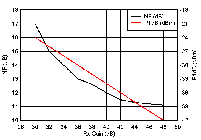
Figure 7-1 shows variations of noise figure and in-band P1dB parameters with respect to receiver gain programmed.
 Figure 7-1 Noise Figure, In-band P1dB vs Receiver
Gain