ZHCSCZ0F June 2014 – March 2017 AMC1305L25 , AMC1305M05 , AMC1305M25
PRODUCTION DATA.
- 1 特性
- 2 应用
- 3 说明
- 4 修订历史记录
- 5 Device Comparison Table
- 6 Pin Configuration and Functions
-
7 Specifications
- 7.1 Absolute Maximum Ratings
- 7.2 ESD Ratings
- 7.3 Recommended Operating Conditions
- 7.4 Thermal Information
- 7.5 Power Ratings
- 7.6 Insulation Specifications
- 7.7 Safety-Related Certifications
- 7.8 Safety Limiting Values
- 7.9 Electrical Characteristics: AMC1305M05
- 7.10 Electrical Characteristics: AMC1305x25
- 7.11 Switching Characteristics
- 7.12 Insulation Characteristics Curves
- 7.13 Typical Characteristics
- 8 Detailed Description
- 9 Application and Implementation
- 10Power-Supply Recommendations
- 11Layout
- 12器件和文档支持
- 13机械、封装和可订购信息
8 Detailed Description
8.1 Overview
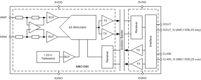
The differential analog input (AINP and AINN) of the AMC1305 is a fully-differential amplifier feeding the switched-capacitor input of a second-order delta-sigma (ΔΣ) modulator stage that digitizes the input signal into a 1-bit output stream. The isolated data output (DOUT) of the converter provides a stream of digital ones and zeros synchronous to the externally-provided clock source at the CLKIN pin with a frequency in the range of 5 MHz to 20.1 MHz. The time average of this serial bit-stream output is proportional to the analog input voltage.
The Functional Block Diagram section shows a detailed block diagram of the AMC1305. The analog input range is tailored to directly accommodate a voltage drop across a shunt resistor used for current sensing. The SiO2-based capacitive isolation barrier supports a high level of magnetic field immunity as described in the application report ISO72x Digital Isolator Magnetic-Field Immunity (SLLA181A), available for download at www.ti.com. The external clock input simplifies the synchronization of multiple current-sense channels on the system level. The extended frequency range of up to 20.1 MHz supports higher performance levels compared to other solutions available on the market.
8.2 Functional Block Diagram

8.3 Feature Description
8.3.1 Analog Input
The AMC1305 incorporates front-end circuitry that contains a differential amplifier and sampling stage, followed by a ΔΣ modulator. The gain of the differential amplifier is set by internal precision resistors to a factor of 4 for devices with a specified input voltage range of ±250 mV (for the AMC1305x25), or to a factor of 20 for devices with a ±50-mV input voltage range (for the AMC1305M05), resulting in a differential input impedance of 5 kΩ (for the AMC1305M05) or 25 kΩ (for the AMC1305x25).
Consider the input impedance of the AMC1305 in designs with high-impedance signal sources that can cause degradation of gain and offset specifications. The importance of this effect, however, depends on the desired system performance. Additionally, the input bias current caused by the internal common-mode voltage at the output of the differential amplifier causes an offset that depends on the actual amplitude of the input signal. See the Isolated Voltage Sensing section for more details on reducing these effects.
There are two restrictions on the analog input signals (AINP and AINN). First, if the input voltage exceeds the range of AGND – 6 V to AVDD + 0.5 V, the input current must be limited to 10 mA because the device input electrostatic discharge (ESD) protection diodes turn on. In addition, the linearity and noise performance of the device are ensured only when the differential analog input voltage remains within the specified linear full-scale range (FSR), that is ±250 mV (for the AMC1305x25) or ±50 mV (for the AMC1305M05), and within the specified input common-mode range.
8.3.2 Modulator
The modulator implemented in the AMC1305 is a second-order, switched-capacitor, feed-forward ΔΣ modulator, such as the one conceptualized in Figure 48. The analog input voltage VIN and the output V5 of the 1-bit digital-to-analog converter (DAC) are differentiated, providing an analog voltage V1 at the input of the first integrator stage. The output of the first integrator feeds the input of the second integrator stage, resulting in output voltage V3 that is differentiated with the input signal VIN and the output of the first integrator V2. Depending on the polarity of the resulting voltage V4, the output of the comparator is changed. In this case, the 1-bit DAC responds on the next clock pulse by changing its analog output voltage V5, causing the integrators to progress in the opposite direction while forcing the value of the integrator output to track the average value of the input.
 Figure 48. Block Diagram of a Second-Order Modulator
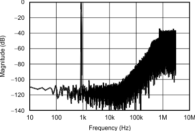
The modulator shifts the quantization noise to high frequencies; see Figure 49. Therefore, use a low-pass digital filter at the output of the device to increase overall performance. This filter is also used to convert from the 1-bit data stream at a high sampling rate into a higher-bit data word at a lower rate (decimation). TI's microcontroller family TMS320F2837x offers a suitable programmable, hardwired filter structure termed a sigma-delta filter module (SDFM) optimized for usage with the AMC1305 family. Also, SD24_B converters on the MSP430F677x microcontrollers offer a path to directly access the integrated sinc-filters, thus offering a system-level solution for multichannel isolated current sensing. An additional option is to use a suitable application-specific device (such as the AMC1210, a four-channel digital sinc-filter). Alternatively, a field-programmable gate array (FPGA) can be used to implement the digital filter.

8.3.3 Digital Output
A differential input signal of 0 V ideally produces a stream of ones and zeros that are high 50% of the time. A differential input of 250 mV (for the AMC1305x25) or 50 mV (for the AMC1305M05) produces a stream of ones and zeros that are high 90% of the time. A differential input of –250 mV (–50 mV for the AMC1305M05) produces a stream of ones and zeros that are high 10% of the time. These input voltages are also the specified linear ranges of the different AMC1305 versions with performance as specified in this document. If the input voltage value exceeds these ranges, the output of the modulator shows non-linear behavior while the quantization noise increases. The output of the modulator would clip with a stream of only zeros with an input less than or equal to –312.5 mV (–62.5 mV for the AMC1305M05) or with a stream of only ones with an input greater than or equal to 312.5 mV (62.5 mV for the AMC1305M05). In this case, however, the AMC1305 generates a single 1 (if the input is at negative full-scale) or 0 every 128 clock cycles to indicate proper device function (see the Fail-Safe Output section for more details). The input voltage versus the output modulator signal is shown in Figure 50.
The density of ones in the output bit-stream for any input voltage value (with the exception of a full-scale input signal as described in Output Behavior in Case of Full-Scale Input ) can be calculated using Equation 1:

The AMC1305 system clock is typically 20 MHz and is provided externally at the CLKIN pin. Data are synchronously provided at 20 MHz at the DOUT pin. Data change at the CLKIN falling edge. For more details, see the Switching Characteristics table.
 Figure 50. Analog Input versus AMC1305 Modulator Output
8.4 Device Functional Modes
8.4.1 Fail-Safe Output
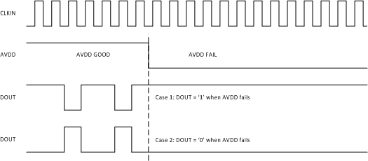
In the case of a missing high-side supply voltage (AVDD), the output of a ΔΣ modulator is not defined and could cause a system malfunction. In systems with high safety requirements, this behavior is not acceptable. Therefore, the AMC1305 implements a fail-safe output function that ensures the device maintains its output level in case of a missing AVDD, as shown in Figure 51.
 Figure 51. Fail-Safe Output of the AMC1305
8.4.2 Output Behavior in Case of Full-Scale Input
If a full-scale input signal is applied to the AMC1305 (that is, VIN ≥ VClipping), the device generates a single one or zero every 128 bits at DOUT, depending on the actual polarity of the signal being sensed, as shown in Figure 52.
In this way, differentiating between a missing AVDD and a full-scale input signal is possible on the system level.
 Figure 52. Overrange Output of the AMC1305