ZHCSIP8B August   2018  – April 2020 AMC1035

PRODUCTION DATA.  

  1. 特性
  2. 应用
  3. 说明
    1.     Device Images
      1.      应用示例
  4. 修订历史记录
  5. Pin Configuration and Functions
    1.     Pin Functions
  6. Specifications
    1. 6.1 Absolute Maximum Ratings
    2. 6.2 ESD Ratings
    3. 6.3 Recommended Operating Conditions
    4. 6.4 Thermal Information
    5. 6.5 Electrical Characteristics
    6. 6.6 Switching Characteristics
    7. 6.7 Typical Characteristics
  7. Detailed Description
    1. 7.1 Overview
    2. 7.2 Functional Block Diagram
    3. 7.3 Feature Description
      1. 7.3.1 Analog Input
      2. 7.3.2 Modulator
      3. 7.3.3 Reference Output
      4. 7.3.4 Clock Input
      5. 7.3.5 Digital Output
      6. 7.3.6 Manchester Coding Feature
    4. 7.4 Device Functional Modes
      1. 7.4.1 Output Behavior in Case of a Full-Scale Input
      2. 7.4.2 Fail-Safe Output
  8. Application and Implementation
    1. 8.1 Application Information
      1. 8.1.1 Digital Filter Usage
    2. 8.2 Typical Applications
      1. 8.2.1 Voltage Sensing
        1. 8.2.1.1 Design Requirements
        2. 8.2.1.2 Detailed Design Procedure
        3. 8.2.1.3 Application Curve
      2. 8.2.2 IGBT Temperature Sensing
      3. 8.2.3 What to Do and What Not to Do
  9. Power Supply Recommendations
  10. 10Layout
    1. 10.1 Layout Guidelines
    2. 10.2 Layout Example
  11. 11器件和文档支持
    1. 11.1 文档支持
      1. 11.1.1 相关文档
    2. 11.2 接收文档更新通知
    3. 11.3 社区资源
    4. 11.4 商标
    5. 11.5 静电放电警告
    6. 11.6 Glossary
  12. 12机械、封装和可订购信息

封装选项

机械数据 (封装 | 引脚)
散热焊盘机械数据 (封装 | 引脚)
订购信息

Analog Input

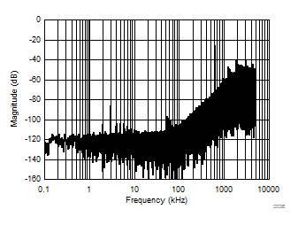
The AMC1035 incorporates front-end circuitry that contains a buffered sampling stage, followed by a ΔΣ modulator. To support a bipolar input range, the device uses a charge pump that allows single-supply operation to simplify the overall system design and minimize the circuit cost. For reduced offset and offset drift, the input buffer is chopper-stabilized with the switching frequency set at fCLKIN / 32. Figure 37 shows the spur created by the switching frequency.
AMC1035 D036_SBAS837.gif
sinc3 filter, OSR = 2, fCLKIN = 20 MHz, fIN = 1 kHz
Figure 37. Quantization Noise Shaping

The linearity and noise performance of the device are ensured only when the differential analog input voltage remains within the specified linear full-scale range (FSR), that is ±1 V, and within the specified input common-mode range.

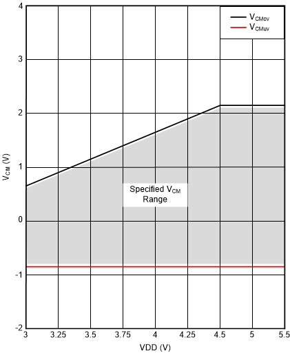
Figure 38 shows the specified common-mode input voltage that applies for the full-scale input voltage range as specified in this document along with the corresponding common-mode undervoltage and overvoltage threshold levels.

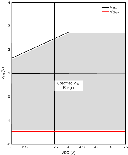
If smaller input signals are used, the operational common-mode input voltage range widens. Figure 39 shows the common-mode input voltage that applies with no differential input signal; that is, when the voltage applied on AINP is equal to the voltage applied on AINN. The common-mode input voltage range scales with the actual differential input voltage between this range and the range in Figure 38.
AMC1035 ai_Vcm_FS_bas837.gif
Figure 38. Common-Mode Input Voltage Range With a
Full-Scale Differential Input Signal of ±1.25 V
AMC1035 ai_Vcm_no_input_bas837.gif
Figure 39. Common-Mode Input Voltage Range With a
Zero Differential Input Signal