ZHCSFS8A December 2016 – April 2017 ADS8588S
PRODUCTION DATA.
- 1 特性
- 2 应用
- 3 说明
- 4 修订历史记录
- 5 Device Family Comparison Table
- 6 Pin Configuration and Functions
-
7 Specifications
- 7.1 Absolute Maximum Ratings
- 7.2 ESD Ratings
- 7.3 Recommended Operating Conditions
- 7.4 Thermal Information
- 7.5 Electrical Characteristics
- 7.6 Timing Requirements: CONVST Control
- 7.7 Timing Requirements: Data Read Operation
- 7.8 Timing Requirements: Parallel Data Read Operation, CS and RD Tied Together
- 7.9 Timing Requirements: Parallel Data Read Operation, CS and RD Separate
- 7.10 Timing Requirements: Serial Data Read Operation
- 7.11 Timing Requirements: Byte Mode Data Read Operation
- 7.12 Timing Requirements: Oversampling Mode
- 7.13 Timing Requirements: Exit Standby Mode
- 7.14 Timing Requirements: Exit Shutdown Mode
- 7.15 Switching Characteristics: CONVST Control
- 7.16 Switching Characteristics: Parallel Data Read Operation, CS and RD Tied Together
- 7.17 Switching Characteristics: Parallel Data Read Operation, CS and RD Separate
- 7.18 Switching Characteristics: Serial Data Read Operation
- 7.19 Switching Characteristics: Byte Mode Data Read Operation
- 7.20 Typical Characteristics
-
8 Detailed Description
- 8.1 Overview
- 8.2 Functional Block Diagram
- 8.3 Feature Description
- 8.4
Device Functional Modes
- 8.4.1
Device Interface: Pin Description
- 8.4.1.1 REFSEL (Input)
- 8.4.1.2 RANGE (Input)
- 8.4.1.3 STBY (Input)
- 8.4.1.4 PAR/SER/BYTE SEL (Input)
- 8.4.1.5 CONVSTA, CONVSTB (Input)
- 8.4.1.6 RESET (Input)
- 8.4.1.7 RD/SCLK (Input)
- 8.4.1.8 CS (Input)
- 8.4.1.9 OS[2:0]
- 8.4.1.10 BUSY (Output)
- 8.4.1.11 FRSTDATA (Output)
- 8.4.1.12 DB15/BYTE SEL
- 8.4.1.13 DB14/HBEN
- 8.4.1.14 DB[13:9]
- 8.4.1.15 DB8/DOUTB
- 8.4.1.16 DB7/DOUTA
- 8.4.1.17 DB[6:0]
- 8.4.2 Device Modes of Operation
- 8.4.1
Device Interface: Pin Description
- 9 Application and Implementation
- 10Power Supply Recommendations
- 11Layout
- 12器件和文档支持
- 13机械、封装和可订购信息
10 Power Supply Recommendations
The ADS8588S uses two separate power supplies: AVDD and DVDD. The AVDD supply provides power to the ADC and internal circuits, and DVDD is used for the digital interface. AVDD and DVDD can be set independently to voltages within the permissible range.
The AVDD supply can be set in the range of 4.75 V to 5.25 V. A low-noise, linear regulator is recommended to generate the analog supply voltage. The device has four AVDD pins. Each AVDD pin must be decoupled with respect to AGND using a 1-µF capacitor. Place the 1-µF capacitor as close to the supply pins as possible.
The DVDD supply is used to drive the digital I/O buffers and can be set in the range of 2.3 V to a maximum value equal to the AVDD voltage. This range allows the device to interface with most state-of-the-art processors and controllers. Place a 1-µF (minimum 100-nF) decoupling capacitor in close proximity to the DVDD supply to provide the high-frequency digital switching current.
There are no specific requirements with regard to the power-supply sequencing of the device. However, issue a reset after the supplies are powered and are stable to ensure the device is properly configured.
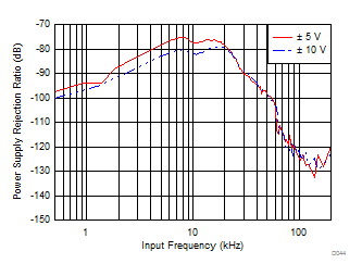
The typical PSRR curve with the decoupling capacitors is as shown in Figure 88.
