SBAS482C January 2010 – September 2017 ADS7924
PRODUCTION DATA.
- 1 Features
- 2 Applications
- 3 Description
- 4 Revision History
- 5 Pin Configuration and Functions
- 6 Specifications
- 7 Detailed Description
-
8 Application and Implementation
- 8.1
Application Information
- 8.1.1 Using an Operational Amplifier Between Multiplexer Output and ADC Input
- 8.1.2 Using an Operational Amplifier and RC Filter Between Multiplexer Output and ADC Input
- 8.1.3 Using an RC Filter Between Multiplexer Output and ADC Input
- 8.1.4 Operational Amplifier With Filter and Gain Option Between Multiplexer Output and ADC Input
- 8.1.5 Driving an RC Filter With an Operational Amplifier Between Multiplexer Output and ADC Input
- 8.1.6 Average Power Consumption
- 8.2 Typical Application
- 8.1
Application Information
- 9 Power Supply Recommendations
- 10Layout
- 11Device and Documentation Support
- 12Mechanical, Packaging, and Orderable Information
10 Layout
10.1 Layout Guidelines
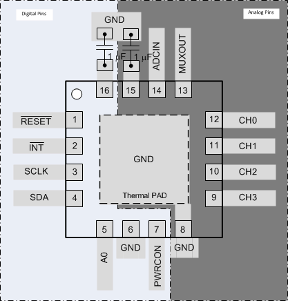
Figure 65 provides an example layout for the device. Use a ground plane underneath the device and partition the PCB into analog and digital sections. Avoid crossing digital lines with the analog signal path and keep the analog input signals and the reference input signals away from noise sources. In Figure 65, the analog signals are routed on the rightside of the device and the digital signals are routed on the left side of the device.
The power sources to the device must be clean and well-bypassed. Use 1-μF ceramic bypass capacitors in close proximity to the analog (AVDD) and digital (DVDD) power-supply pins. Avoid placing vias between the AVDD and DVDD pins and the bypass capacitors. Connect all ground pins to the ground plane using short, low-impedance paths. The AVDD supply voltage for the device also functions as a reference for the device. Place the decoupling capacitor for AVDD close to the device AVDD pin and connect this capacitor to the device pins with thick copper tracks.
10.2 Layout Example
 Figure 65. Example Layout