ZHCSCM5B October   2013  – August 2014 ADS7254 , ADS7854 , ADS8354

PRODUCTION DATA.  

  1. 特性
  2. 应用
  3. 说明
  4. 修订历史记录
  5. Device Comparison Table
  6. Pin Configurations and Functions
  7. Specifications
    1. 7.1  Absolute Maximum Ratings
    2. 7.2  Handling Ratings
    3. 7.3  Recommended Operating Conditions
    4. 7.4  Thermal Information
    5. 7.5  Electrical Characteristics: ADS8354
    6. 7.6  Electrical Characteristics: ADS7854
    7. 7.7  Electrical Characteristics: ADS7254
    8. 7.8  Electrical Characteristics: All Devices
    9. 7.9  Timing Requirements: Interface Mode
    10. 7.10 Timing Characteristics: Serial Interface
    11. 7.11 Typical Characteristics: ADS8354
    12. 7.12 Typical Characteristics: ADS7854
    13. 7.13 Typical Characteristics: ADS7254
    14. 7.14 Typical Characteristics: Common to ADS8354, ADS7854, and ADS7254
  8. Detailed Description
    1. 8.1 Overview
    2. 8.2 Functional Block Diagram
    3. 8.3 Feature Description
      1. 8.3.1 Reference
      2. 8.3.2 Analog Inputs
        1. 8.3.2.1 Analog Input: Full-Scale Range Selection
        2. 8.3.2.2 Analog Input: Common-Mode Voltage Range
      3. 8.3.3 Transfer Function
    4. 8.4 Device Functional Modes
    5. 8.5 Register Maps and Serial Interface
      1. 8.5.1 Serial Interface
      2. 8.5.2 Write to User Programmable Registers
        1. 8.5.2.1 Configuration Register (CFR)
        2. 8.5.2.2 REFDAC Registers (REFDAC_A and REFDAC_B)
      3. 8.5.3 Data Read Operation
        1. 8.5.3.1 Reading User-Programmable Registers
        2. 8.5.3.2 Conversion Data Read
          1. 8.5.3.2.1 32-CLK, Dual-SDO Mode (CFR.B11 = 0, CFR.B10 = 0, Default)
          2. 8.5.3.2.2 32-CLK, Single-SDO Mode (CFR.B11 = 0, CFR.B10 = 1)
          3. 8.5.3.2.3 16-CLK, Dual-SDO Mode (CFR.B11 = 1, CFR.B10 = 0)
          4. 8.5.3.2.4 16-CLK, Single-SDO Mode (CFR.B11 = 1, CFR.B10 = 1)
      4. 8.5.4 Low-Power Modes
        1. 8.5.4.1 STANDBY Mode
        2. 8.5.4.2 Software Power-Down (SPD) Mode
      5. 8.5.5 Frame Abort, Reconversion, or Short-Cycling
  9. Application and Implementation
    1. 9.1 Application Information
      1. 9.1.1 Input Amplifier Selection
      2. 9.1.2 Antialiasing Filter
    2. 9.2 Typical Applications
      1. 9.2.1 DAQ Circuit to Achieve Maximum SINAD for a 10-kHz Input Signal at Full Throughput
        1. 9.2.1.1 Design Requirements
        2. 9.2.1.2 Detailed Design Procedure
        3. 9.2.1.3 Application Curves
      2. 9.2.2 DAQ Circuit to Achieve Maximum SINAD for a 100-kHz Input Signal at Full Throughput
        1. 9.2.2.1 Design Requirements
        2. 9.2.2.2 Detailed Design Procedure
        3. 9.2.2.3 Application Curves
  10. 10Power-Supply Recommendations
  11. 11Layout
    1. 11.1 Layout Guidelines
    2. 11.2 Layout Example
  12. 12器件和文档支持
    1. 12.1 相关链接
    2. 12.2 相关文档 
    3. 12.3 Trademarks
    4. 12.4 Electrostatic Discharge Caution
    5. 12.5 术语表
  13. 13机械封装和可订购信息

封装选项

机械数据 (封装 | 引脚)
散热焊盘机械数据 (封装 | 引脚)
订购信息

10 Power-Supply Recommendations

The devices have two separate power supplies: AVDD and DVDD. The device operates on AVDD; DVDD is used for the interface circuits. AVDD and DVDD can be independently set to any value within the permissible ranges.

When using the device with ±2 × VREF input range (CFR.B9 = 1), the AVDD supply voltage value defines the permissible voltage swing on the analog input pins. To avoid saturation of output codes, and to use the full dynamic range on the analog input pins, AVDD must be set as shown in Equation 11, Equation 12, and Equation 13:

Equation 11. AVDD ≥ 2 × VREF_A
Equation 12. AVDD ≥ 2 × VREF_B
Equation 13. 4.75 V ≤ AVDD ≤ 5.25 V

Decouple the AVDD and DVDD pins with the GND pin using individual 10-µF decoupling capacitors, as shown in Figure 115.

ai_supply_bas584.gif
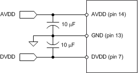
Figure 115. Power-Supply Decoupling