ZHCSAV9B April 2013 – January 2016 ADS5401
PRODUCTION DATA.
- 1 特性
- 2 应用
- 3 说明
- 4 修订历史记录
- 5 Device Options
- 6 Pin Configuration and Functions
-
7 Specifications
- 7.1 Absolute Maximum Ratings
- 7.2 ESD Ratings
- 7.3 Recommended Operating Conditions
- 7.4 Thermal Information
- 7.5 Electrical Characteristics - Supply, Power Supply
- 7.6 Electrical Characteristics - Analog Inputs, Dynamic Accuracy, Clock Input
- 7.7 Electrical Characteristics - Dynamic AC, Enabled
- 7.8 Electrical Characteristics- Dynamic AC, Disabled
- 7.9 Electrical Characteristics - Over-Drive Recovery Error, Sample Timing
- 7.10 Electrical Characteristics - Digital Inputs, Digital Outputs
- 7.11 Serial Register Write Timing Requirements
- 7.12 Reset Timing Requirements
- 7.13 Typical Characteristics
-
8 Detailed Description
- 8.1 Overview
- 8.2 Functional Block Diagram
- 8.3 Feature Description
- 8.4 Device Functional Modes
- 8.5 Programming
- 8.6
Register Maps
- 8.6.1 Register Name: Config0 - Address: 0×00, Default = 0×00
- 8.6.2 Register Name: Config1 - Address: 0×01, Default = 0×00
- 8.6.3 Register Name: Config2 - Address: 0×02, Default = 0×780
- 8.6.4 Register Name: 3 - Address: 0x03
- 8.6.5 Register Name: E - Address: 0x0E
- 8.6.6 Register Name: F - Address: 0x0F
- 8.6.7 Register Name: 2B - Address: 0x2B
- 8.6.8 Register Name: 2C - Address: 0x2C
- 8.6.9 Register Name: 37 - Address: 0x37
- 8.6.10 Register Name: 38 - Address: 0x38
- 8.6.11 Register Name: 3A - Address: 0x3A
- 8.6.12 Register Name: 66 - Address: 0x66
- 9 Application and Implementation
- 10Power Supply Recommendations
- 11Layout
- 12器件和文档支持
- 13机械、封装和可订购信息
7 Specifications
7.1 Absolute Maximum Ratings
over operating free-air temperature range (unless otherwise noted)(1)| MIN | MAX | UNIT | ||
|---|---|---|---|---|
| Supply voltage | AVDD33 | –0.5 | 4 | V |
| AVDDC | –0.5 | 2.3 | ||
| AVDD18 | –0.5 | 2.3 | ||
| DVDD | –0.5 | 2.3 | ||
| DVDDLVDS | –0.5 | 2.3 | ||
| IOVDD | –0.5 | 4 | ||
| Voltage applied to input pins | INA_P, INA_N | –0.5 | AVDD33 + 0.5 | V |
| CLKINP, CLKINN | –0.5 | AVDDC + 0.5 | V | |
| SYNCP, SYNCN | –0.5 | AVDD33 + 0.5 | V | |
| SRESET, SDENB, SCLK, SDIO, SDO, ENABLE | –0.5 | IOVDD + 0.5 | V | |
| Operating free-air temperature, TA | –40 | 85 | °C | |
| Operating junction temperature, TJ | 150 | °C | ||
| Storage temperature, Tstg | –65 | 150 | °C | |
(1) Stresses beyond those listed under Absolute Maximum Ratings may cause permanent damage to the device. These are stress ratings only, which do not imply functional operation of the device at these or any other conditions beyond those indicated under Recommended Operating Conditions. Exposure to absolute-maximum-rated conditions for extended periods may affect device reliability.
7.2 ESD Ratings
| VALUE | UNIT | |||
|---|---|---|---|---|
| V(ESD) | Electrostatic discharge | Human-body model (HBM), per ANSI/ESDA/JEDEC JS-001 (1) | 2000 | V |
| Charged-device model (CDM), per JEDEC specification JESD22-C101 (2) | 750 | |||
(1) JEDEC document JEP155 states that 500-V HBM allows safe manufacturing with a standard ESD control process.
(2) JEDEC document JEP157 states that 250-V CDM allows safe manufacturing with a standard ESD control process.
7.3 Recommended Operating Conditions
over operating free-air temperature range (unless otherwise noted)| MIN | NOM | MAX | UNIT | |||
|---|---|---|---|---|---|---|
| SUPPLY | ||||||
| Supply voltage | AVDD33 | 3.15 | 3.3 | 3.45 | V | |
| AVDDC, AVDD18, DVDD, DVDDLVDS | 1.7 | 1.8 | 1.9 | |||
| IOVDD | 1.7 | 1.8 | 3.45 | |||
| GENERAL PARAMETERS | ||||||
| ADC Clock Frequency | 40 | 800 | MSPS | |||
| Resolution | 12 | Bits | ||||
| TJ | Recommended operating junction temperature | 105 | °C | |||
| Maximum rated operating junction temperature(1) | 125 | |||||
| TA | Recommended free-air temperature | –40 | 25 | 85 | °C | |
(1) Prolonged use at this junction temperature may increase the device failure-in-time (FIT) rate.
7.4 Thermal Information
| THERMAL METRIC(1) | ADS5401 | UNIT | |
|---|---|---|---|
| ZAY (NFBGA) | |||
| 196 PINS | |||
| RθJA | Junction-to-ambient thermal resistance(2) | 37.6 | °C/W |
| RθJC(top) | Junction-to-case (top) thermal resistance(3) | 6.8 | °C/W |
| RθJB | Junction-to-board thermal resistance(4) | 16.8 | °C/W |
| ψJT | Junction-to-top characterization parameter(5) | 0.2 | °C/W |
| ψJB | Junction-to-board characterization parameter(6) | 16.4 | °C/W |
| RθJC(bot) | Junction-to-case (bottom) thermal resistance(7) | N/A | °C/W |
(1) For more information about traditional and new thermal metrics, see the Semiconductor and IC Package Thermal Metrics application report (SPRA953).
(2) The junction-to-ambient thermal resistance under natural convection is obtained in a simulation on a JEDEC-standard, high-K board, as specified in JESD51-7, in an environment described in JESD51-2a.
(3) The junction-to-case (top) thermal resistance is obtained by simulating a cold plate test on the package top. No specific JEDEC-standard test exists, but a close description can be found in the ANSI SEMI standard G30-88.
(4) The junction-to-board thermal resistance is obtained by simulating in an environment with a ring cold plate fixture to control the PCB temperature, as described in JESD51-8.
(5) The junction-to-top characterization parameter, ψJT, estimates the junction temperature of a device in a real system and is extracted from the simulation data for obtaining RθJA, using a procedure described in JESD51-2a (sections 6 and 7).
(6) The junction-to-board characterization parameter, ψJB, estimates the junction temperature of a device in a real system and is extracted from the simulation data for obtaining RθJA, using a procedure described in JESD51-2a (sections 6 and 7).
(7) The junction-to-case (bottom) thermal resistance is obtained by simulating a cold plate test on the exposed (power) pad. No specific JEDEC standard test exists, but a close description can be found in the ANSI SEMI standard G30-88.
Spacer
Spacer
7.5 Electrical Characteristics - Supply, Power Supply
Typical values at TA = 25°C, full temperature range is TMIN = –40°C to TMAX = 85 °C, ADC sampling rate = 800 Msps, 50% clock duty cycle, AVDD33 = 3.3V, AVDDC/AVDD18/DVDD/DVDDLVDS/IOVDD = 1.8 V, –1 dBFS differential input (unless otherwise noted).| PARAMETER | TEST CONDITIONS | MIN | TYP | MAX | UNIT | |
|---|---|---|---|---|---|---|
| POWER SUPPLY | ||||||
| IAVDD33 | 3.3-V analog supply current | 161 | 181 | mA | ||
| IAVDD18 | 1.8-V analog supply current | 73 | 85 | mA | ||
| IAVDDC | 1.8-V clock supply current | 52 | 70 | mA | ||
| IDVDD | 1.8-V digital supply current | Auto correction enabled | 238 | 280 | mA | |
| IDVDD | 1.8-V digital supply current | Auto correction disabled | 175 | mA | ||
| IDVDD | 1.8-V digital supply current | Auto correction disabled, decimation filter enabled | 190 | mA | ||
| IDVDDLVDS | 1.8-V LVDS supply current | 80 | 100 | mA | ||
| IIOVDD | 1.8-V I/O Voltage supply current | 1 | 2 | mA | ||
| Pdis | Total power dissipation | Auto correction enabled, decimation filter disabled | 1.33 | 1.6 | W | |
| Pdis | Total power dissipation | Auto correction disabled, decimation filter disabled | 1.22 | W | ||
| PSRR | 250kHz to 500MHz | 40 | dB | |||
| Shut-down power dissipation | 7 | mW | ||||
| Shut-down wake-up time | 2.5 | ms | ||||
| Standby power dissipation | 7 | mW | ||||
| Standby wake-up time | 100 | µs | ||||
| Deep-sleep mode power dissipation | Auto correction disabled | 295 | mW | |||
| Auto correction enabled | 360 | mW | ||||
| Deep-sleep mode wake-up time | 20 | µs | ||||
| Light-sleep mode power dissipation | Auto correction disabled | 465 | mW | |||
| Auto correction enabled | 530 | mW | ||||
| Light-sleep mode wake-up time | 2 | µs | ||||
7.6 Electrical Characteristics - Analog Inputs, Dynamic Accuracy, Clock Input
Typical values at TA = 25°C, full temperature range is TMIN = –40°C to TMAX = 85°C, ADC sampling rate = 800 Msps, 50% clock duty cycle, AVDD3V = 3.3V, AVDD/DRVDD/IOVDD = 1.8 V, –1 dBFS differential input (unless otherwise noted).| PARAMETER | TEST CONDITIONS | MIN | TYP | MAX | UNIT |
|---|---|---|---|---|---|
| ANALOG INPUTS | |||||
| Differential input full-scale | 1.0 | Vpp | |||
| Input common-mode voltage | 1.9 | ±0.1 | V | ||
| Input resistance | Differential at DC | 1 | kΩ | ||
| Input capacitance | Each input to GND | 2 | pF | ||
| VCM common-mode voltage output | 1.9 | V | |||
| Analog input bandwidth (3dB) | 1200 | MHz | |||
| DYNAMIC ACCURACY | |||||
| Offset Error | Auto correction disabled | –20 | ±6 | 20 | mV |
| Auto correction enabled | –1 | 0 | 1 | mV | |
| Offset temperature coefficient | –10 | µV/°C | |||
| Gain error | –5 | ±0.6 | 5 | %FS | |
| Gain temperature coefficient | 0.003 | %FS/°C | |||
| Differential nonlinearity | fIN = 230 MHz | –1 | ±0.8 | 2 | LSB |
| Integral nonlinearity | fIN = 230 MHz | -5 | ±2 | 5 | LSB |
| CLOCK INPUT | |||||
| Input clock frequency | 40 | 800 | MHz | ||
| Input clock amplitude | 2 | Vpp | |||
| Input clock duty cycle | 40% | 50% | 60% | ||
| Internal clock biasing | 0.9 | V | |||
7.7 Electrical Characteristics - Dynamic AC, Enabled
Typical values at TA = 25°C, full temperature range is TMIN = –40°C to TMAX = 85°C, ADC sampling rate = 800 Msps, 50% clock duty cycle, AVDD33 = 3.3V, AVDDC / AVDD18 / DVDD / DVDDLVDS / IOVDD = 1.8 V, –1 dBFS differential input (unless otherwise noted).| PARAMETER | TEST CONDITIONS | MIN | TYP | MAX | UNIT | |
|---|---|---|---|---|---|---|
| Auto Correction | Enabled | Vpp | ||||
| DYNAMIC AC CHARACTERISTICS(1) | ||||||
| SNR | Signal-to-Noise Ratio | fIN = 10 MHz | 61.7 | dBFS | ||
| fIN = 100 MHz | 61.7 | |||||
| fIN = 230 MHz | 58 | 61.3 | ||||
| fIN = 450 MHz | 60.7 | |||||
| fIN = 700 MHz | 59.8 | |||||
| HD2,3 | Second and third harmonic distortion | fIN = 10 MHz | 78 | dBc | ||
| fIN = 100 MHz | 77 | |||||
| fIN = 230 MHz | 67 | 77 | ||||
| fIN = 450 MHz | 76 | |||||
| fIN = 700 MHz | 74 | |||||
| Non HD2,3 | Spur free dynamic range (excluding second and third harmonic distortion Fs/2 – FIN spur) |
fIN = 10 MHz | 81 | dBc | ||
| fIN = 100 MHz | 79 | |||||
| fIN = 230 MHz | 67 | 78 | ||||
| fIN = 450 MHz | 78 | |||||
| fIN = 700 MHz | 76 | |||||
| IL | Fs/2-Fin interleaving spur | fIN = 10 MHz | 91 | dBc | ||
| fIN = 100 MHz | 81 | |||||
| fIN = 230 MHz | 63 | 74 | ||||
| fIN = 450 MHz | 72 | |||||
| fIN = 700 MHz | 69 | |||||
| SINAD | Signal-to-noise and distortion ratio | fIN = 10 MHz | 61.6 | dBFS | ||
| fIN = 100 MHz | 61.4 | |||||
| fIN = 230 MHz | 57.7 | 61 | ||||
| fIN = 450 MHz | 60.5 | |||||
| fIN = 700 MHz | 59.5 | |||||
| THD | Total Harmonic Distortion | fIN = 10 MHz | 75 | dBc | ||
| fIN = 100 MHz | 73 | |||||
| fIN = 230 MHz | 66 | 73 | ||||
| fIN = 450 MHz | 74 | |||||
| fIN = 700 MHz | 72 | |||||
| IMD3 | Inter modulation distortion | Fin = 169.5 and 170.5 MHz, -7dBFS |
76 | dBFS | ||
| Fin = 649.5 and 650.5 MHz, -7dBFS |
70 | |||||
| Crosstalk | 90 | dB | ||||
| ENOB | Effective number of bits | fIN = 230 MHz | 9.8 | LSB | ||
(1) SFDR and SNR calculations do not include the DC or Fs/2 bins when Auto Correction is disabled.
7.8 Electrical Characteristics- Dynamic AC, Disabled
over operating free-air temperature range (unless otherwise noted)| PARAMETER | TEST CONDITIONS | MIN | TYP | MAX | UNIT | |
|---|---|---|---|---|---|---|
| Auto correction | Disabled | Vpp | ||||
| DYNAMIC AC CHARACTERISTICS (1) | ||||||
| SNR | Signal to Noise Ratio | fIN = 10 MHz | 61.8 | dBFS | ||
| fIN = 100 MHz | 61.8 | |||||
| fIN = 230 MHz | 61.5 | |||||
| fIN = 450 MHz | 61.1 | |||||
| fIN = 700 MHz | 60.6 | |||||
| HD2,3 | Second and third harmonic distortion | fIN = 10 MHz | 80 | dBc | ||
| fIN = 100 MHz | 77 | |||||
| fIN = 230 MHz | 79 | |||||
| fIN = 450 MHz | 77 | |||||
| fIN = 700 MHz | 75 | |||||
| Non HD2,3 | Spur Free Dynamic Range (excluding second and third harmonic distortion Fs/2 – FIN spur) |
fIN = 10 MHz | 83 | dBc | ||
| fIN = 100 MHz | 81 | |||||
| fIN = 230 MHz | 79 | |||||
| fIN = 450 MHz | 79 | |||||
| fIN = 700 MHz | 77 | |||||
| IL | Fs/2-Fin interleaving spur | fIN = 10 MHz | 84 | dBc | ||
| fIN = 100 MHz | 80 | |||||
| fIN = 230 MHz | 75 | |||||
| fIN = 450 MHz | 71 | |||||
| fIN = 700 MHz | 69 | |||||
| SINAD | Signal to noise and distortion ratio | fIN = 10 MHz | 61.7 | dBFS | ||
| fIN = 100 MHz | 61.6 | |||||
| fIN = 230 MHz | 61.3 | |||||
| fIN = 450 MHz | 61 | |||||
| fIN = 700 MHz | 60.3 | |||||
| THD | Total Harmonic Distortion | fIN = 10 MHz | 77 | dBc | ||
| fIN = 100 MHz | 75 | |||||
| fIN = 230 MHz | 74 | |||||
| fIN = 450 MHz | 75 | |||||
| fIN = 700 MHz | 72 | |||||
| IMD3 | Inter modulation distortion | Fin = 169.5 and 170.5 MHz, -7dBFS |
76 | dBFS | ||
| Fin = 649.5 and 650.5 MHz, -7dBFS |
72 | |||||
| Crosstalk | 90 | dB | ||||
| ENOB | Effective number of bits | fIN = 230 MHz | 9.8 | LSB | ||
7.9 Electrical Characteristics - Over-Drive Recovery Error, Sample Timing
Typical values at TA = 25°C, full temperature range is TMIN = –40°C to TMAX = 85°C, ADC sampling rate = 800Msps, 50% clock duty cycle, AVDD33 = 3.3 V, AVDDC/AVDD18/DVDD/DVDDLVDS/IOVDD = 1.8 V, –1 dBFS differential input (unless otherwise noted).| PARAMETER | TEST CONDITIONS | MIN | TYP | MAX | UNIT | |
|---|---|---|---|---|---|---|
| OVER-DRIVE RECOVERY ERROR | ||||||
| Input overload recovery | Recovery to within 1% (of final value) for 6dB overload with sine wave input | 2 | Output Clock | |||
| SAMPLE TIMING CHARACTERISTICS | ||||||
| Aperture Jitter | Sample uncertainty | 100 | fs rms | |||
| Data Latency | ADC sample to digital output, auto correction disabled | 38 | Clock Cycles | |||
| ADC sample to digital output, auto correction enabled | 50 | |||||
| ADC sample to digital output, Decimation filter enabled, Auto correction disabled | 74 | Sampling Clock Cycles | ||||
| Over-range Latency | ADC sample to over-range output | 12 | Clock Cycles | |||
7.10 Electrical Characteristics - Digital Inputs, Digital Outputs
The DC specifications refer to the condition where the digital outputs are not switching, but are permanently at a valid logic level 0 or 1. AVDD33 = 3.3 V, AVDDC/AVDD18/DVDD/DVDDLVDS/IOVDD = 1.8 V| PARAMETER | TEST CONDITIONS | MIN | TYP | MAX | UNIT | |
|---|---|---|---|---|---|---|
| DIGITAL INPUTS – SRESET, SCLK, SDENB, SDIO, ENABLE | ||||||
| High-level input voltage | All digital inputs support 1.8-V and 3.3-V logic levels. | 0.7 x IOVDD | V | |||
| Low-level input voltage | 0.3 x IOVDD | V | ||||
| High-level input current | –50 | 200 | µA | |||
| Low-level input current | –50 | 50 | µA | |||
| Input capacitance | 5 | pF | ||||
| DIGITAL OUTPUTS – SDO | ||||||
| High-level output voltage | Iload = -100 µA | IOVDD – 0.2 | V | |||
| Iload = -2 mA | 0.8 x IOVDD | |||||
| Low-level output voltage | Iload = 100 µA | 0.2 | V | |||
| Iload = 2 mA | 0.22 x IOVDD | |||||
| DIGITAL INPUTS – SYNCP/N | ||||||
| VID | Differential input voltage | 250 | 350 | 450 | mV | |
| VCM | Input common-mode voltage | 1.125 | 1.2 | 1.375 | V | |
| tSU | 500 | ps | ||||
| DIGITAL OUTPUTS – DA[11:0]P/N, DACLKP/N, OVRAP/N, SYNCOUTP/N | ||||||
| VOD | Output differential voltage | IOUT = 3.5 mA | 250 | 350 | 450 | mV |
| VOCM | Output common-mode voltage | IOUT = 3.5 mA | 1.125 | 1.25 | 1.375 | V |
| tsu | Fs = 800 Msps, Data valid to zero-crossing of DACLK | 230 | 450 | ps | ||
| th | Fs = 800 Msps, Zero-crossing of DACLK to data becoming invalid | 230 | 410 | ps | ||
| tPD | Fs = 800 Msps, CLKIN falling edge to DACLK, DBCLK rising edge | 3.36 | 3.69 | 3.92 | ns | |
| tRISE | 10% - 90% | 100 | 150 | 200 | ps | |
| tFALL | 90% - 10% | 100 | 150 | 200 | ps | |
7.11 Serial Register Write Timing Requirements
| MIN | MAX | UNIT | ||
|---|---|---|---|---|
| fSCLK | SCLK frequency (equal to 1/tSCLK) | > DC | 20 | MHz |
| tSLOADS | SDENB to SCLK setup time | 25 | ns | |
| tSLOADH | SCLK to SDENB hold time | 25 | ns | |
| tDSU | SDIO setup time | 25 | ns | |
| tDH | SDIO hold time | 25 | ns | |
7.12 Reset Timing Requirements
| MIN | NOM | MAX | UNIT | |||
|---|---|---|---|---|---|---|
| t1 | Power-on delay | Delay from power up to active low RESET pulse | 3 | ms | ||
| t2 | Reset pulse width | Active low RESET pulse width | 20 | ns | ||
| t3 | Register write delay | Delay from RESET disable to SDENb active | 100 | ns | ||
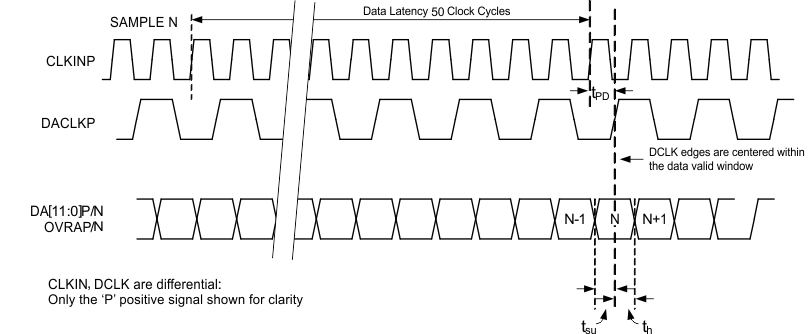 Figure 1. Timing Diagram for 12-Bit DDR Output
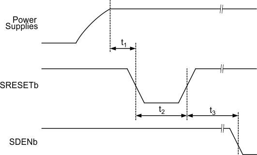 Figure 2. Device Initialization Timing Diagram
7.13 Typical Characteristics
Typical values at TA = +25°C, full temperature range is TMIN = -40°C to TMAX = +85°C, ADC sampling rate = 800 Msps, 50% clock duty cycle, AVDD33 = 3.3 V, AVDDC /AVDD18 / DVDD / DVDDLVDS / IOVDD = 1.8 V, -1dBFS differential input, unless otherwise noted.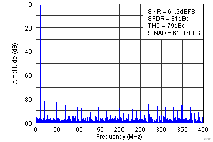 Figure 3. FFT for 10-MHz Input Signal (Auto On)
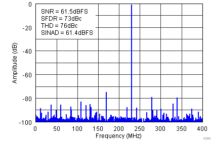 Figure 5. FFT for 230-MHz Input Signal (Auto On)
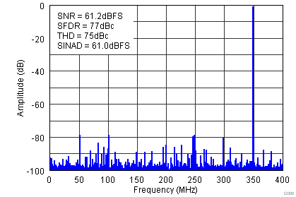 Figure 7. FFT for 450-MHz Input Signal (Auto On)
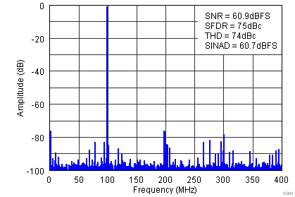 Figure 9. FFT for 700-MHz Input Signal (Auto On)
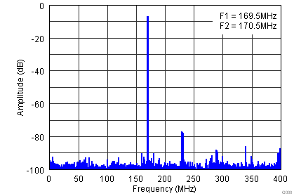 Figure 11. FFT for Two Tone Input Signal (Auto On)
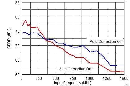 Figure 13. SFDR vs Input Frequency
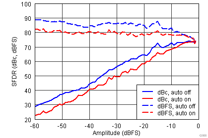 Figure 15. SFDR vs Amplitude (fin = 230 MHz)
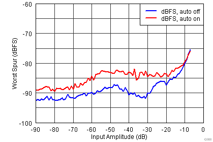 Figure 17. Tow Tone Performance Across Input Amplitude
(fin = 170 MHz)
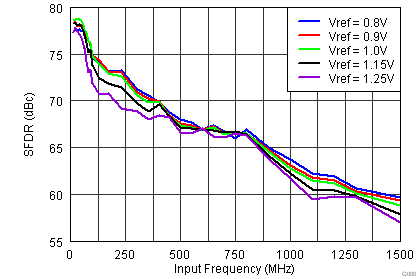 Figure 19. SFDR vs Vref (Auto Off)
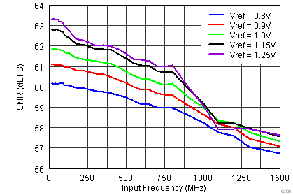 Figure 21. SNR vs Vref (Auto Off)
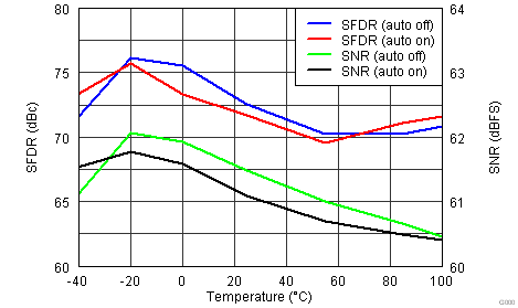 Figure 23. Performance Across Temperature (fin = 230 MHz)
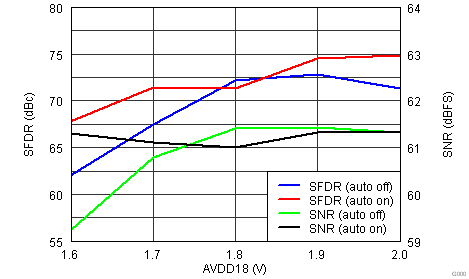 Figure 25. Performance Across AVDD18 (fin = 230MHz)
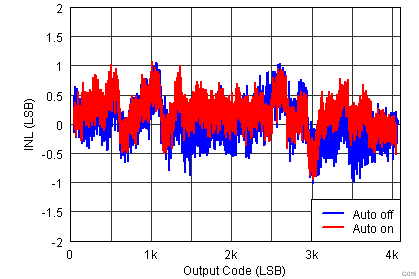 Figure 27. INL
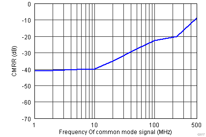 Figure 29. CMRR Across Frequency
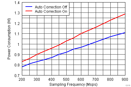 Figure 31. Power Across Sampling Frequency
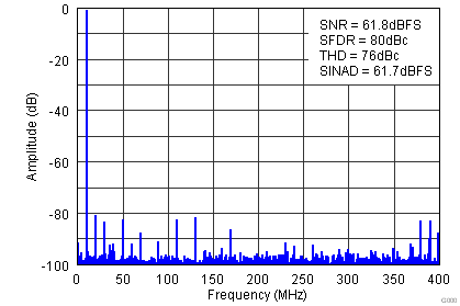 Figure 4. FFT for 10-MHz Input Signal (Auto Off)
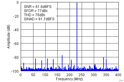 Figure 6. FFT for 230-MHz Input Signal (Auto Off)
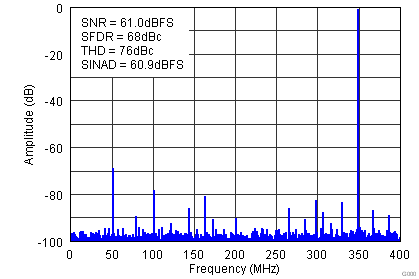 Figure 8. FFT for 450-MHz Input Signal (Auto Off)
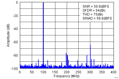 Figure 10. FFT for 700-MHz Input Signal (Auto Off)
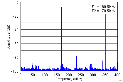 Figure 12. FFT for Two Tone Input Signal (Auto Off)
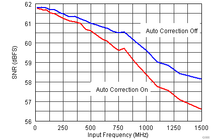 Figure 14. SNR vs Input Frequency
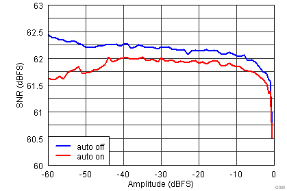 Figure 16. SNR vs Amplitude (fin = 230 MHz)
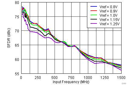 Figure 18. SFDR vs Vref (Auto On)
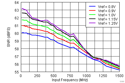 Figure 20. SNR vs Vref (Auto On)
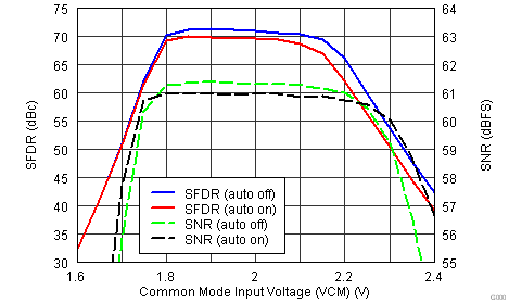 Figure 22. Performance Across Input
Common-Mode Voltage (fin = 230 MHz)
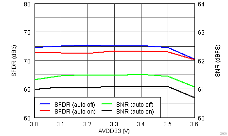 Figure 24. Performance Across AVDD33 (fin = 230 MHz)
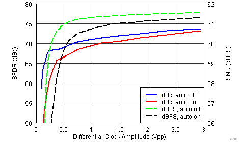 Figure 26. Performance Across Clock Amplitude
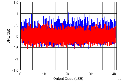 Figure 28. DNL
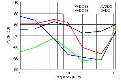 Figure 30. PSRR Across Frequency
.png) Figure 32. SFDR Across Input and Sampling Frequencies (Auto On)
Figure 32. SFDR Across Input and Sampling Frequencies (Auto On)
.png) Figure 34. SNR Across Input and Sampling Frequencies (Auto On)
Figure 34. SNR Across Input and Sampling Frequencies (Auto On)
.png) Figure 33. SFDR Across Input and Sampling Frequencies (Auto Off)
Figure 33. SFDR Across Input and Sampling Frequencies (Auto Off)
.png) Figure 35. SNR Across Input and Sampling Frequencies (Auto On)
Figure 35. SNR Across Input and Sampling Frequencies (Auto On)