ZHCS146C December 2011 – April 2020 ADS1291 , ADS1292 , ADS1292R
PRODUCTION DATA.
- 1 特性
- 2 应用
- 3 说明
- 4 修订历史记录
- 5 Pin Configuration and Functions
- 6 Specifications
- 7 Parameter Measurement Information
-
8 Detailed Description
- 8.1 Overview
- 8.2 Functional Block Diagram
- 8.3
Feature Description
- 8.3.1 EMI Filter
- 8.3.2
Input Multiplexer
- 8.3.2.1 Device Noise Measurements
- 8.3.2.2 Test Signals (TestP and TestN)
- 8.3.2.3 Auxiliary Differential Input (RESP_MODN/IN3N, RESP_MODN/IN3P)
- 8.3.2.4 Temperature Sensor (TEMPP, TEMPN)
- 8.3.2.5 Supply Measurements (MVDDP, MVDDN)
- 8.3.2.6 Lead-Off Excitation Signals (LoffP, LoffN)
- 8.3.2.7 Auxiliary Single-Ended Input
- 8.3.3 Analog Input
- 8.3.4 PGA Settings and Input Range
- 8.3.5 Digital Decimation Filter
- 8.3.6 Reference
- 8.3.7 Clock
- 8.3.8 Data Format
- 8.3.9 Multiple Device Configuration
- 8.3.10 ECG-Specific Functions
- 8.3.11 Setting the Device for Basic Data Capture
- 8.4 Device Functional Modes
- 8.5
Programming
- 8.5.1 SPI Interface
- 8.5.2
SPI Command Definitions
- 8.5.2.1 WAKEUP: Exit STANDBY Mode
- 8.5.2.2 STANDBY: Enter STANDBY Mode
- 8.5.2.3 RESET: Reset Registers to Default Values
- 8.5.2.4 START: Start Conversions
- 8.5.2.5 STOP: Stop Conversions
- 8.5.2.6 OFFSETCAL: Channel Offset Calibration
- 8.5.2.7 RDATAC: Read Data Continuous
- 8.5.2.8 SDATAC: Stop Read Data Continuous
- 8.5.2.9 RDATA: Read Data
- 8.5.2.10 Sending Multi-Byte Commands
- 8.5.2.11 RREG: Read From Register
- 8.5.2.12 WREG: Write to Register
- 8.6
Register Maps
- 8.6.1
User Register Description
- 8.6.1.1 ID: ID Control Register (Factory-Programmed, Read-Only) (address = 00h)
- 8.6.1.2 CONFIG1: Configuration Register 1 (address = 01h)
- 8.6.1.3 CONFIG2: Configuration Register 2 (address = 02h)
- 8.6.1.4 LOFF: Lead-Off Control Register (address = 03h)
- 8.6.1.5 CH1SET: Channel 1 Settings (address = 04h)
- 8.6.1.6 CH2SET: Channel 2 Settings (address = 05h)
- 8.6.1.7 RLD_SENS: Right Leg Drive Sense Selection (address = 06h)
- 8.6.1.8 LOFF_SENS: Lead-Off Sense Selection (address = 07h)
- 8.6.1.9 LOFF_STAT: Lead-Off Status (address = 08h)
- 8.6.1.10 RESP1: Respiration Control Register 1 (address = 09h)
- 8.6.1.11 RESP2: Respiration Control Register 2 (address = 0Ah)
- 8.6.1.12 GPIO: General-Purpose I/O Register (address = 0Bh)
- 8.6.1
User Register Description
- 9 Application and Implementation
- 10Power Supply Recommendations
- 11Layout
- 12器件和文档支持
- 13机械、封装和可订购信息
封装选项
机械数据 (封装 | 引脚)
散热焊盘机械数据 (封装 | 引脚)
订购信息
8.3.7 Clock
The ADS1291, ADS1292, and ADS1292R provide two different methods for device clocking: internal and external. Internal clocking is ideally suited for low-power, battery-powered systems. The internal oscillator is trimmed for accuracy at room temperature. Over the specified temperature range the accuracy varies; see the Electrical Characteristics. Clock selection is controlled by the CLKSEL pin and the CLK_EN register bit.
The CLKSEL pin selects either the internal or external clock. The CLK_EN bit in the CONFIG2 register enables and disables the oscillator clock to be output in the CLK pin. A truth table for these two pins is shown in Table 9. The CLK_EN bit is useful when multiple devices are used in a daisy-chain configuration. It is recommended that during power-down the external clock be shut down to save power.
Table 9. CLKSEL Pin and CLK_EN Bit
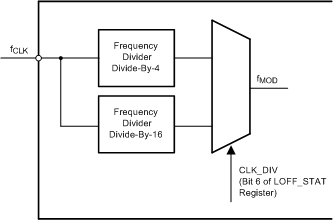
The ADS1291, ADS1292, and ADS1292R have the option to choose between two different external clock frequencies (512 kHz or 2.048 MHz). This frequency is selected by setting the CLK_DIV bit (bit 6) in the LOFF_STAT register. The modulator must be clocked at 128 kHz, regardless of the external clock frequency. Figure 32 shows the relationship between the external clock (fCLK) and the modulator clock (fMOD). The default mode of operation is fCLK = 512 kHz. The higher frequency option has been provided to allow the SPI to run at a higher speed. SCLK can be only twice the speed of fCLK during a register read or write, see section on sending multi-byte commands. Having the 2.048 MHz option allows for register read and writes to be performed at SCLK speeds up to 4.096 MHz.
 Figure 32. Relationship Between External Clock (fCLK) and Modulator Clock (fMOD)