ZHCSII0A July   2018  – November 2018 ADS1219

PRODUCTION DATA.  

  1. 特性
  2. 应用
  3. 说明
    1.     Device Images
      1.      电压、电流和温度监控应用
  4. 修订历史记录
  5. Pin Configuration and Functions
    1.     Pin Functions
  6. Specifications
    1. 6.1 Absolute Maximum Ratings
    2. 6.2 ESD Ratings
    3. 6.3 Recommended Operating Conditions
    4. 6.4 Thermal Information
    5. 6.5 Electrical Characteristics
    6. 6.6 I2C Timing Requirements
    7. 6.7 I2C Switching Characteristics
    8. 6.8 Typical Characteristics
  7. Parameter Measurement Information
    1. 7.1 Noise Performance
  8. Detailed Description
    1. 8.1 Overview
    2. 8.2 Functional Block Diagram
    3. 8.3 Feature Description
      1. 8.3.1 Multiplexer
      2. 8.3.2 Rail-to-Rail Input Buffers and Programmable Gain Stage
      3. 8.3.3 Voltage Reference
      4. 8.3.4 Modulator and Internal Oscillator
      5. 8.3.5 Digital Filter
      6. 8.3.6 Conversion Times
      7. 8.3.7 Offset Calibration
    4. 8.4 Device Functional Modes
      1. 8.4.1 Power-Up and Reset
        1. 8.4.1.1 Power-On Reset
        2. 8.4.1.2 RESET Pin
        3. 8.4.1.3 Reset by Command
      2. 8.4.2 Conversion Modes
        1. 8.4.2.1 Single-Shot Conversion Mode
        2. 8.4.2.2 Continuous Conversion Mode
      3. 8.4.3 Power-Down Mode
    5. 8.5 Programming
      1. 8.5.1 I2C Interface
        1. 8.5.1.1 I2C Address
        2. 8.5.1.2 Serial Clock (SCL) and Serial Data (SDA)
        3. 8.5.1.3 Data Ready (DRDY)
        4. 8.5.1.4 Interface Speed
        5. 8.5.1.5 Data Transfer Protocol
        6. 8.5.1.6 I2C General Call (Software Reset)
        7. 8.5.1.7 Timeout
      2. 8.5.2 Data Format
      3. 8.5.3 Commands
        1. 8.5.3.1 Command Latching
        2. 8.5.3.2 RESET (0000 011x)
        3. 8.5.3.3 START/SYNC (0000 100x)
        4. 8.5.3.4 POWERDOWN (0000 001x)
        5. 8.5.3.5 RDATA (0001 xxxx)
        6. 8.5.3.6 RREG (0010 0rxx)
        7. 8.5.3.7 WREG (0100 00xx dddd dddd)
      4. 8.5.4 Reading Data and Monitoring for New Conversion Results
    6. 8.6 Register Map
      1. 8.6.1 Configuration and Status Registers
      2. 8.6.2 Register Descriptions
        1. 8.6.2.1 Configuration Register (address = 0h) [reset = 00h]
          1. Table 10. Configuration Register Field Descriptions
        2. 8.6.2.2 Status Register (address = 1h) [reset = 00h]
          1. Table 11. Status Register Field Descriptions
  9. Application and Implementation
    1. 9.1 Application Information
      1. 9.1.1 Interface Connections
      2. 9.1.2 Connecting Multiple Devices on the Same I2C Bus
      3. 9.1.3 Unused Inputs and Outputs
      4. 9.1.4 Analog Input Filtering
      5. 9.1.5 External Reference and Ratiometric Measurements
      6. 9.1.6 Establishing Proper Limits on the Absolute Input Voltage
      7. 9.1.7 Pseudo Code Example
    2. 9.2 Typical Application
      1. 9.2.1 Design Requirements
      2. 9.2.2 Detailed Design Procedure
        1. 9.2.2.1 Voltage Monitoring
        2. 9.2.2.2 High-Side Current Measurement
        3. 9.2.2.3 Thermistor Measurement
        4. 9.2.2.4 Register Settings
      3. 9.2.3 Application Curve
  10. 10Power Supply Recommendations
    1. 10.1 Power-Supply Sequencing
    2. 10.2 Power-Supply Decoupling
  11. 11Layout
    1. 11.1 Layout Guidelines
    2. 11.2 Layout Example
  12. 12器件和文档支持
    1. 12.1 器件支持
      1. 12.1.1 第三方产品免责声明
    2. 12.2 文档支持
      1. 12.2.1 相关文档
    3. 12.3 接收文档更新通知
    4. 12.4 社区资源
    5. 12.5 商标
    6. 12.6 静电放电警告
    7. 12.7 术语表
  13. 13机械、封装和可订购信息

封装选项

机械数据 (封装 | 引脚)
散热焊盘机械数据 (封装 | 引脚)
订购信息

Digital Filter

The device uses a linear-phase finite impulse response (FIR) digital filter that performs both filtering and decimation of the digital data stream coming from the modulator. The digital filter is automatically adjusted for the different data rates and always settles within a single cycle. The frequency responses of the digital filter are shown in Figure 28 to Figure 32 for different output data rates. The filter notches and output data rate scale proportionally with the clock frequency. The internal oscillator can vary over temperature as specified in the Electrical Characteristics table. The data rate or conversion time, respectively, and consequently also the filter notches vary proportionally.
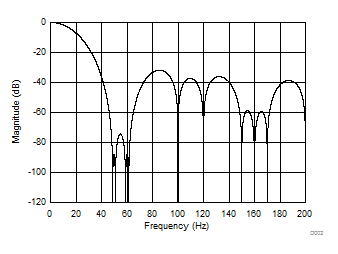
ADS1219 D002.gifFigure 28. Filter Response
(DR = 20 SPS)
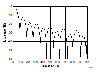
ADS1219 D004.gifFigure 30. Filter Response
(DR = 90 SPS)
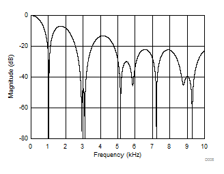
ADS1219 D008_sbas751.gifFigure 32. Filter Response
(DR = 1 kSPS)
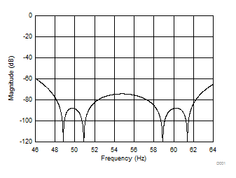
ADS1219 D001.gifFigure 29. Detailed View of the Filter Response
(DR = 20 SPS)
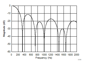
ADS1219 D006.gifFigure 31. Filter Response
(DR = 330 SPS)