ZHCSQQ1B june 2022 – august 2023 ADC32RF54 , ADC32RF55
PRODUCTION DATA
- 1
- 1 特性
- 2 应用
- 3 说明
- 4 Revision History
- 5 Pin Configuration and Functions
-
6 Specifications
- 6.1 Absolute Maximum Ratings
- 6.2 ESD Ratings
- 6.3 Recommended Operating Conditions
- 6.4 Thermal Information
- 6.5 Electrical Characteristics - Power Consumption
- 6.6 Electrical Characteristics - DC Specifications
- 6.7 Electrical Characteristics - ADC32RF54 AC Specifications (Dither DISABLED)
- 6.8 Electrical Characteristics - ADC32RF54 AC Specifications (Dither ENABLED)
- 6.9 Electrical Characteristics - ADC32RF55 AC Specifications (Dither DISABLED)
- 6.10 Electrical Characteristics - ADC32RF55 AC Specifications (Dither ENABLED)
- 6.11 Timing Requirements
- 6.12 Typical Characteristics - ADC32RF54
- 6.13 Typical Characteristics - ADC32RF55
-
7 Detailed Description
- 7.1 Overview
- 7.2 Functional Block Diagram
- 7.3
Feature Description
- 7.3.1 Analog Inputs
- 7.3.2 Sampling Clock Input
- 7.3.3 SYSREF
- 7.3.4 ADC Foreground Calibration
- 7.3.5 Decimation Filter
- 7.3.6
JESD204B Interface
- 7.3.6.1 JESD204B Initial Lane Alignment (ILA)
- 7.3.6.2 JESD204B Frame Assembly
- 7.3.6.3 JESD204B Frame Assembly in Bypass Mode
- 7.3.6.4 JESD204B Frame Assembly with Complex Decimation - Single Band
- 7.3.6.5 JESD204B Frame Assembly with Real Decimation - Single Band
- 7.3.6.6 JESD204B Frame Assembly with Complex Decimation - Dual Band
- 7.3.6.7 JESD204B Frame Assembly with Complex Decimation - Quad Band
- 7.3.7 SERDES Output MUX
- 7.3.8 Test Pattern
- 7.4 Device Functional Modes
- 7.5 Programming
- 7.6 Register Maps
-
8 Application and Implementation
- 8.1 Application Information
- 8.2 Typical Applications
- 8.3
Initialization Set Up
- 8.3.1
Initial Device Configuration After Power-Up
- 8.3.1.1 STEP 1: RESET
- 8.3.1.2 STEP 2: Device Configuration
- 8.3.1.3 STEP 3: JESD Interface Configuration (1)
- 8.3.1.4 STEP 4: SYSREF Synchronization
- 8.3.1.5 STEP 5: JESD Interface Configuration (2)
- 8.3.1.6 STEP 6: Analog Trim Settings
- 8.3.1.7 STEP 7: Calibration Configuration
- 8.3.1.8 STEP 8: SYSREF Synchronization
- 8.3.1.9 STEP 9: Run Power up Calibration
- 8.3.1.10 STEP 10: JESD Interface Synchronization
- 8.3.1
Initial Device Configuration After Power-Up
- 8.4 Power Supply Recommendations
- 8.5 Layout
- 9 Device and Documentation Support
- 10Mechanical, Packaging, and Orderable Information
8.3 Initialization Set Up
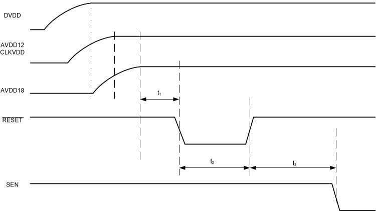
After power-up, the internal registers must be initialized to their default values through a hardware reset by applying a low pulse on the RESET pin, as shown in Figure 8-4.
- Apply 1.2 V DVDD digital power supply
- Apply remaining 1.2 V power supplies (AVDD12, CLKVDD), in no specific order
- Apply 1.8 V AVDD18 power supply
- Apply hardware reset. After hardware reset is released, the default registers are loaded from internal fuses.
- Begin programming the internal registers using the SPI interface.
 Figure 8-4 Initialization of Serial Registers After Power-Up
Table 8-2 Power-Up Timing
| MIN | TYP | MAX | UNIT | ||
|---|---|---|---|---|---|
| t1 | Power-on delay: delay from power up to active high RESET pulse | 1 | ms | ||
| t2 | Reset pulse width: active low RESET pulse width | 100 | ns | ||
| t3 | Register write delay: delay from RESET disable to SEN active | 45k | Clock cycles | ||