SNAS411P August 2008 – April 2017 ADC128S102QML-SP
PRODUCTION DATA.
- 1 Features
- 2 Applications
- 3 Description
- 4 Revision History
- 5 Pin Configuration and Functions
-
6 Specifications
- 6.1 Absolute Maximum Ratings
- 6.2 ESD Ratings
- 6.3 Recommended Operating Conditions
- 6.4 Thermal Information
- 6.5 Electrical Characteristics: ADC128S102QML-SP Converter
- 6.6 Electrical Characteristics: Radiation
- 6.7 Electrical Characteristics: Burn in Delta Parameters - TA at 25°C
- 6.8 Timing Requirements
- 6.9 Typical Characteristics
- 7 Detailed Description
- 8 Application and Implementation
- 9 Power Supply Recommendations
- 10Layout
- 11Device and Documentation Support
- 12Mechanical, Packaging, and Orderable Information
封装选项
请参考 PDF 数据表获取器件具体的封装图。
机械数据 (封装 | 引脚)
- NAC|16
- Y|0
- NAD|16
散热焊盘机械数据 (封装 | 引脚)
订购信息
8 Application and Implementation
NOTE
Information in the following applications sections is not part of the TI component specification, and TI does not warrant its accuracy or completeness. TI’s customers are responsible for determining suitability of components for their purposes. Customers should validate and test their design implementation to confirm system functionality.
8.1 Application Information
The ADC128S102 device is a low-power, eight-channel 12-bit ADC with ensured performance specifications from 50 kSPS to 1 MSPS. It is appropriate to utilize the ADC128S102 at sample rates below 50 kSPS by powering the device down (de-asserting CSB) in between conversions. The Electrical Characteristics information highlights the clock frequency where the ADC’s performance is ensured. There is no limitation on periods of time for shutdown between conversions.
8.2 Typical Application
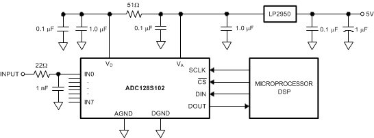
A typical application is shown in Figure 38. The split analog and digital supply pins are both powered in this example by the Texas Instruments LP2950-N low-dropout voltage regulator. The analog supply is bypassed with a capacitor network located close to the ADC128S102. The digital supply is separated from the analog supply by an isolation resistor and bypassed with additional capacitors. The ADC128S102 uses the analog supply (VA) as its reference voltage, so it is very important that VA be kept as clean as possible. Due to the low power requirements of the ADC128S102, it is also possible to use a precision reference as a power supply.
 Figure 38. Typical Application Circuit
8.2.1 Design Requirements
A positive supply only data acquisition system capable of digitizing up to eight single-ended input signals ranging from 0 to 5 V with BW = 10 kHz and a throughput up to 500 kSPS. The ADC128S102 has to interface to an MCU whose supply is set at 5 V. If it is necessary to interface with an MCU that operates at 3.3 V or lower, VA and VD will need to be separated and care must be taken to ensure that VA is powered before VD.
8.2.2 Detailed Design Procedure
The signal range requirement forces the design to use 5-V analog supply at VA, analog supply. This follows from the fact that VA is also a reference potential for the ADC. If the requirement of interfacing to the MCU changes to 3.3-V, it will be necessary to change the VD supply voltage to 3.3 V. The maximum sampling rate of the ADC128S102 when all channels (eight) are enabled is, Fs = FSCLK / (16 × 8).
Note that faster sampling rates can be achieved when fewer channels are sampled. Single channel can be sampled at the maximum rate of Fs (single) = FSCLK / 16.
The VA and VD pins are separated by a 51-Ω resistor in order to minimize digital noise from corrupting the analog reference input. If additional filtering is required, the resistor can be replaced by a ferrite bead, thus achieving a 2nd-order filter response. Further noise consideration could be given to the SPI interface, especially when the master MCU is capable of producing fast rising edges on the digital bus signals. Inserting small resistances in the digital signal path may help in reducing the ground bounce, and thus improve the overall noise performance of the system. Care should be taken when the signal source is capable of producing voltages beyond VA. In such instances, the internal ESD diodes may start conducting. The ESD diodes are not intended as input signal clamps. To provide the desired clamping action use Schottky diodes.
8.2.3 Application Curve
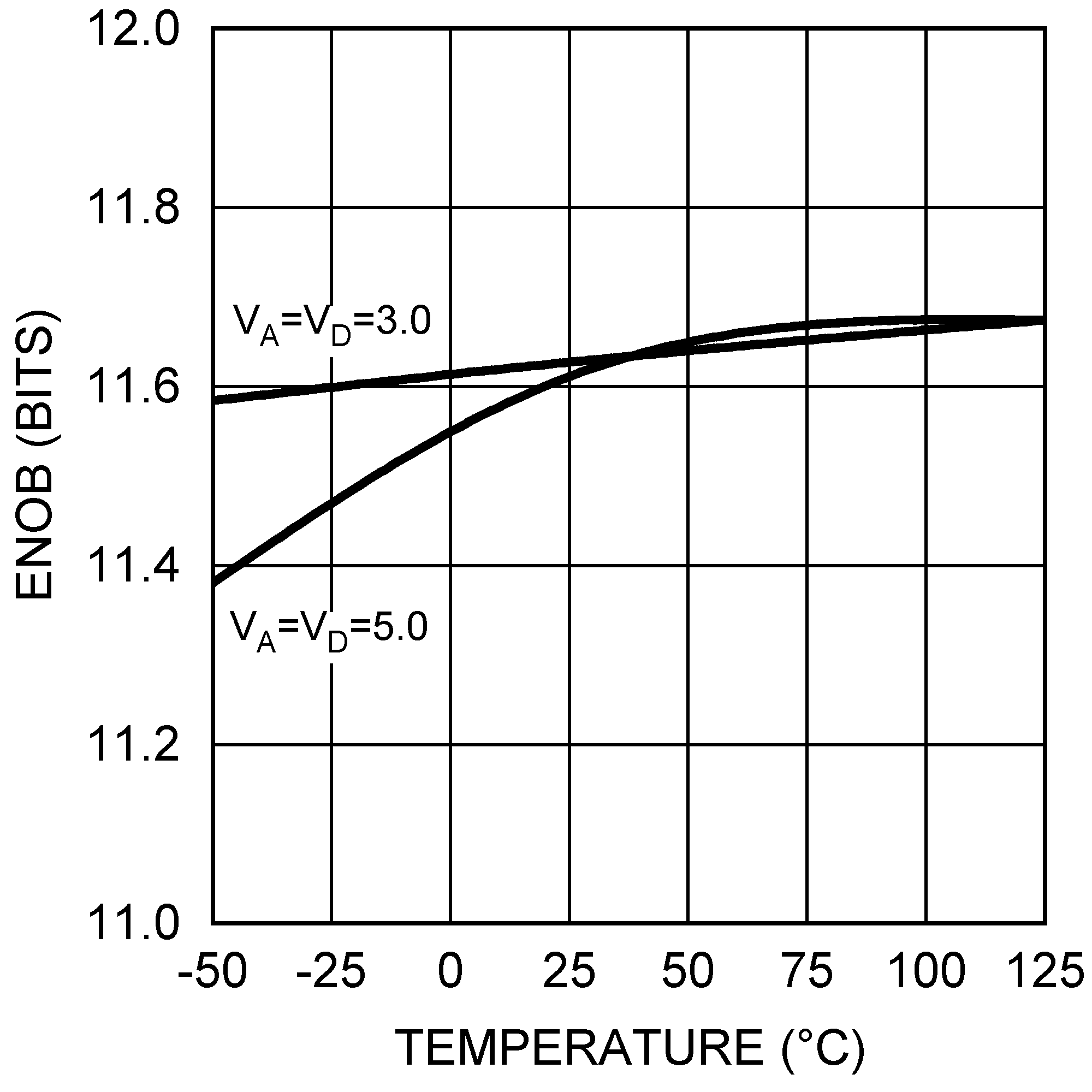
 Figure 39. ENOB vs Temperature