SNAS483F February 2010 – August 2015 ADC128D818
PRODUCTION DATA.
- 1 Features
- 2 Applications
- 3 Description
- 4 Revision History
- 5 Description (continued)
- 6 Pin Configuration and Functions
- 7 Specifications
-
8 Detailed Description
- 8.1 Overview
- 8.2 Functional Block Diagram
- 8.3 Feature Description
- 8.4 Device Functional Modes
- 8.5 Programming
- 8.6
Register Maps
- 8.6.1 ADC128D818 Internal Registers
- 8.6.2 Configuration Register — Address 00h
- 8.6.3 Interrupt Status Register — Address 01h
- 8.6.4 Interrupt Mask Register — Address 03h
- 8.6.5 Conversion Rate Register — Address 07h
- 8.6.6 Channel Disable Register — Address 08h
- 8.6.7 One-Shot Register — Address 09h
- 8.6.8 Deep Shutdown Register — Address 0Ah
- 8.6.9 Advanced Configuration Register — Address 0Bh
- 8.6.10 Busy Status Register — Address 0Ch
- 8.6.11 Channel Readings Registers — Addresses 20h - 27h
- 8.6.12 Limit Registers — Addresses 2Ah - 39h
- 8.6.13 Manufacturer ID Register — Address 3Eh
- 8.6.14 Revision ID Register — Addresses 3Fh
-
9 Application and Implementation
- 9.1 Application Information
- 9.2
Typical Application
- 9.2.1 Design Requirements
- 9.2.2
Detailed Design Procedure
- 9.2.2.1 Power Management
- 9.2.2.2
Using the ADC128D818
- 9.2.2.2.1 Quick Start
- 9.2.2.2.2 Poweron Reset (POR)
- 9.2.2.2.3 Configuration Register (address 00h)
- 9.2.2.2.4 Interrupt Status Register (address 01h)
- 9.2.2.2.5 Interrupt Mask Register (address 03h)
- 9.2.2.2.6 Conversion Rate Register (address 07h)
- 9.2.2.2.7 One-Shot Register (address 09h)
- 9.2.2.2.8 Deep Shutdown Register (address 0Ah)
- 9.2.2.2.9 Channel Readings Registers (addresses 20h - 27h)
- 9.2.3 Application Curve
- 9.3 System Examples
- 10Power Supply Recommendations
- 11Layout
- 12Device and Documentation Support
- 13Mechanical, Packaging, and Orderable Information
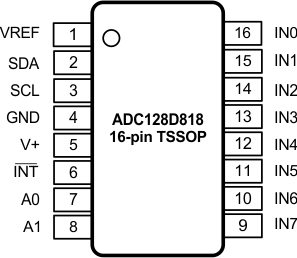
6 Pin Configuration and Functions
PW Package
16-Pin TSSOP
Top View

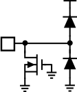
Pin Functions
| PIN | TYPE | DESCRIPTION | ||
|---|---|---|---|---|
| NO. | NAME | ESD STRUCTURE | ||
| 1 | VREF |
 |
Analog Input | ADC external reference. ADC128D818 allows two choices for sourcing VREF: internal or external. If the 2.56-V internal VREF is used, leave this pin unconnected. If the external VREF is used, source this pin with a voltage between 1.25 V and V+. At Power-On-Reset (POR), the default setting is the internal VREF. Bypass with the parallel combination of 1-μF (electrolytic or tantalum) and 0.1-μF (ceramic) capacitors. |
| 2 | SDA |
 |
Digital I/O | Serial Bus Bidirectional Data. NMOS open-drain output. Requires external pullup resistor to function properly. |
| 3 | SCL |
 |
Digital Input | Serial Bus Clock. Requires external pullup resistor to function properly. |
| 4 | GND | GROUND | Internally connected to all of the circuitry. | |
| 5 | V+ |
 |
POWER | 3.0-V to 5.5-V power. Bypass with the parallel combination of 1-μF (electrolytic or tantalum) and 0.1-μF (ceramic) bypass capacitors. |
| 6 | INT |
 |
Digital Output | Interrupt Request. Active Low, NMOS, open-drain. Requires external pullup resistor to function properly. |
| 7 | A0 |
 |
Tri-Level Inputs | Tri-Level Serial Address pins that allow 9 devices on a single I2C bus. |
| 8 | A1 | |||
| 9 | IN7 |
 |
Analog Inputs | The full scale range will be controlled by the internal or external VREF. These inputs can be assigned as single-ended and/or pseudo-differential inputs. |
| 10 | IN6 | |||
| 11 | IN5 | |||
| 12 | IN4 | |||
| 13 | IN3 | |||
| 14 | IN2 | |||
| 15 | IN1 | |||
| 16 | IN0 | |||