SNAS483F February 2010 – August 2015 ADC128D818
PRODUCTION DATA.
- 1 Features
- 2 Applications
- 3 Description
- 4 Revision History
- 5 Description (continued)
- 6 Pin Configuration and Functions
- 7 Specifications
-
8 Detailed Description
- 8.1 Overview
- 8.2 Functional Block Diagram
- 8.3 Feature Description
- 8.4 Device Functional Modes
- 8.5 Programming
- 8.6
Register Maps
- 8.6.1 ADC128D818 Internal Registers
- 8.6.2 Configuration Register — Address 00h
- 8.6.3 Interrupt Status Register — Address 01h
- 8.6.4 Interrupt Mask Register — Address 03h
- 8.6.5 Conversion Rate Register — Address 07h
- 8.6.6 Channel Disable Register — Address 08h
- 8.6.7 One-Shot Register — Address 09h
- 8.6.8 Deep Shutdown Register — Address 0Ah
- 8.6.9 Advanced Configuration Register — Address 0Bh
- 8.6.10 Busy Status Register — Address 0Ch
- 8.6.11 Channel Readings Registers — Addresses 20h - 27h
- 8.6.12 Limit Registers — Addresses 2Ah - 39h
- 8.6.13 Manufacturer ID Register — Address 3Eh
- 8.6.14 Revision ID Register — Addresses 3Fh
-
9 Application and Implementation
- 9.1 Application Information
- 9.2
Typical Application
- 9.2.1 Design Requirements
- 9.2.2
Detailed Design Procedure
- 9.2.2.1 Power Management
- 9.2.2.2
Using the ADC128D818
- 9.2.2.2.1 Quick Start
- 9.2.2.2.2 Poweron Reset (POR)
- 9.2.2.2.3 Configuration Register (address 00h)
- 9.2.2.2.4 Interrupt Status Register (address 01h)
- 9.2.2.2.5 Interrupt Mask Register (address 03h)
- 9.2.2.2.6 Conversion Rate Register (address 07h)
- 9.2.2.2.7 One-Shot Register (address 09h)
- 9.2.2.2.8 Deep Shutdown Register (address 0Ah)
- 9.2.2.2.9 Channel Readings Registers (addresses 20h - 27h)
- 9.2.3 Application Curve
- 9.3 System Examples
- 10Power Supply Recommendations
- 11Layout
- 12Device and Documentation Support
- 13Mechanical, Packaging, and Orderable Information
1 Features
- 12-Bit Resolution Delta-Sigma ADC
- Local Temperature Sensing
- Configurable Single-Ended and/or Pseudo-Diff. Inputs
- 2.56-V Internal VREF or Variable External VREF
- WATCHDOG Window Comparators with Status and Mask Registers of All Measured Values
- Independent Registers for Storing Measured Values
- INT Output Notifies Microprocessor of Error Event
- I2C Serial Bus Interface Compatibility
- 9 Selectable Addresses
- TIME-OUT Reset Function to Prevent I2C Bus Lock-Up
- Individual Channel Shutdown to Limit Power Consumption
- Deep Shutdown Mode to Minimize Power Consumption
- TSSOP 16-Lead Package
- Key Specifications
- ADC Resolution 12-Bit
- Supply Voltage Range 3 V to 5.5 V
- Total Unadjusted Error –0.45%/+0.2%
- Integral Non-Linearity ±1 LSb
- Differential Non-Linearity ±1 LSb
- Operating Current 0.56 mA
- Deep Shutdown Current 10 µA
- Temperature Resolution °C/LSb
- Temperature Accuracy (–40°C to 125°C) ±3°C
- Temperature Accuracy (–25°C to 100°C) ±2°C
2 Applications
- Communications Infrastructure
- Thermal and Hardware Server Monitors
- System Monitors
- Industrial and Medical Systems
- Electronic Test Equipment and Instrumentation
- Power Supply Monitoring and Supervision
3 Description
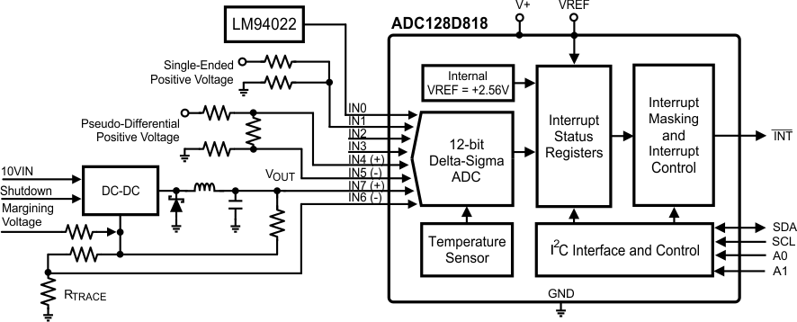
The ADC128D818 I2C system monitor is designed for maximum flexibility. The system monitor can be configured for single-ended and/or pseudo-differential inputs. An onboard temperature sensor, combined with WATCHDOG window comparators, and an interrupt output pin, INT, allow easy monitoring and out-of-range alarms for every channel. A high performance internal reference is also available to provide for a complete solution in the most difficult operating conditions.
The ADC128D818’s 12-bit delta-sigma ADC supports Standard Mode (Sm, 100 kbps) and Fast Mode (Fm, 400 kbps) I2C interfaces. The ADC128D818 includes a sequencer to control channel conversions and stores all converted results in independent registers for easy microprocessor retrieval. Unused channels can be shut down independently to conserve power.
Device Information(1)
| PART NUMBER | PACKAGE | BODY SIZE (NOM) |
|---|---|---|
| ADC128D818 | TSSOP (16) | 5.00 mm × 4.40 mm |
- For all available packages, see the orderable addendum at the end of the data sheet.
Typical Application Diagram
