ZHCSEK0A November 2015 – November 2015 THS4541-Q1
PRODUCTION DATA.
- 1 特性
- 2 应用
- 3 说明
- 4 修订历史记录
- 5 Device Family Comparison
- 6 Pin Configuration and Functions
- 7 Specifications
-
8 Parameter Measurement Information
- 8.1 Example Characterization Circuits
- 8.2 Frequency-Response Shape Factors
- 8.3 I/O Headroom Considerations
- 8.4 Output DC Error and Drift Calculations and the Effect of Resistor Imbalances
- 8.5 Noise Analysis
- 8.6 Factors Influencing Harmonic Distortion
- 8.7 Driving Capacitive Loads
- 8.8 Thermal Analysis
-
9 Detailed Description
- 9.1 Overview
- 9.2 Functional Block Diagram
- 9.3 Feature Description
- 9.4
Device Functional Modes
- 9.4.1
Operation from Single-Ended Sources to Differential Outputs
- 9.4.1.1 AC-Coupled Signal Path Considerations for Single-Ended Input to Differential Output Conversion
- 9.4.1.2 DC-Coupled Input Signal Path Considerations for Single-Ended to Differential Conversion
- 9.4.1.3 Resistor Design Equations for the Single-Ended to Differential Configuration of the FDA
- 9.4.1.4 Input Impedance for the Single-Ended to Differential FDA Configuration
- 9.4.2 Differential-Input to Differential-Output Operation
- 9.4.1
Operation from Single-Ended Sources to Differential Outputs
- 10Application and Implementation
- 11Power-Supply Recommendations
- 12Layout
- 13器件和文档支持
- 14机械、封装和可订购信息
8 Parameter Measurement Information
8.1 Example Characterization Circuits
The THS4541-Q1 offers the advantages of a fully differential amplifier (FDA) design, with the trimmed input offset voltage of a precision op amp. The FDA is an extremely flexible device that provides a purely differential output signal centered on a settable output common-mode level. The primary options revolve around the choices of single-ended or differential inputs, AC-coupled or DC-coupled signal paths, gain targets, and resistor-value selections. The characterizations shown in Figure 1 to Figure 36 focus on single-ended-to-differential designs as the more challenging application requirement. Differential sources can certainly be supported and are often simpler to both implement and analyze.
Because most lab equipment is single-ended, the characterization circuits typically operate with a single-ended, matched, 50-Ω input termination to a differential output at the FDA output pins. That output is then translated back to single-ended through a variety of baluns (or transformers) depending on the test and frequency range. DC-coupled, step-response testing uses two 50-Ω scope inputs with trace math. The starting point for any single-ended-to-differential, AC-coupled characterization plot is shown in Figure 61.
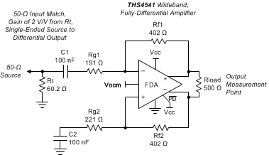 Figure 61. AC-Coupled, Single-Ended Source to a Differential Gain of a 2-V/V Test Circuit
Most characterization plots fix the Rf (Rf1 = Rf2) value at 402 Ω, as shown in Figure 61. This element value is completely flexible in application, but the 402 Ω provides a good compromise for the parasitic issues linked to this value, specifically:
- Added output loading. The FDA appears like an inverting op amp design with both feedback resistors as an added load across the outputs (approximate total differential load in Figure 61 is 500 Ω || 804 Ω = 308 Ω).
- Noise contributions because of the resistor values. The resistors contribute both a 4kTR term and provide gain for the input current noise (see the Noise Analysis section).
- Parasitic feedback pole at the input summing nodes. This pole created by the feedback R value and the
0.85-pF differential input capacitance (as well as any board layout parasitic) introduces a zero in the noise gain, decreasing the phase margin in most situations. This effect must be managed for best frequency response flatness or step response overshoot. The 402-Ω value selected does degrade the phase margin slightly over a lower value, but does not decrease the loading significantly from the nominal 500-Ω value across the output pins.
The frequency domain characterization curves start with the selections of Figure 61. Then, various elements are modified to show their impact over a range of design targets, specifically:
- Gain setting is changed by adjusting Rt and the 2 – Rg elements (holding a 50-Ω input match).
- Output loading, including both resistive and capacitive load testing.
- Power-supply settings. Most often, a single +5-V test uses a ±2.5-V supply, and a +3-V test uses ±1.5-V supplies.
- The disable control pin is tied to Vs+ for any active channel test.
Because most network and spectrum analyzers are a single-ended input, the output network on the THS4541-Q1 characterization tests typically show the desired load connected through a balun to a single-ended, 50-Ω load, while presenting a 50-Ω source from the balun output back into the balun. For instance, Figure 62 shows a wideband MA/Com balun used for Figure 61. This network shows a 500-Ω differential load to the THS4541-Q1, but an AC-coupled, 50-Ω source to the network analyzer. Distortion testing typically uses a lower-frequency, DC-isolated balun (such as the TT1-6T) that is rotated 90° from the wider band interface of Figure 62.
 Figure 62. Example 500-Ω Load to a Single-Ended, Doubly-Terminated, AC-Coupled, 50-Ω Interface
This approach allows a higher differential load, but with a wideband 50-Ω output match at the cost of considerable signal-path insertion loss. This loss is acceptable for characterization, and is normalized out to show the characterization curves.
For time-domain or DC-coupled testing, the circuit of Figure 63 is used as a starting point, where the gain of a
5-V/V setting used in Figure 9 and Figure 27 are illustrated.
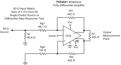 Figure 63. DC-Coupled, Single-Ended-to-Differential, Basic Test Circuit Set for a Gain of 5 V/V
In this case, the input is DC-coupled, showing a 50-Ω input match to the source, gain of 5 V/V to a differential output, again driving a nominal 500-Ω load. Using a single supply, the Vocm control input can either be floated (defaulting to midsupply) or be driven within the allowed range for the Vocm loop (see the headroom limits on Vocm in the Electrical Characteristics tables). To use this circuit for step-response measurements, load each of the two outputs with a 250-Ω network, translating to a 50-Ω source impedance driving into two 50-Ω scope inputs. Then, difference the scope inputs to generate the step responses of Figure 9 and Figure 27. Figure 64 shows the output interface circuit. This grounded interface pulls a DC load current from the output Vocm voltage for single-supply operation. Running this test with balanced bipolar power supplies eliminates this DC load current and gives similar waveform results.
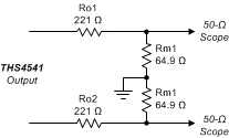 Figure 64. Example 500-Ω Load to Differential, Doubly-Terminated, DC-Coupled 50-Ω Scope Interface
8.2 Frequency-Response Shape Factors
Figure 1 illustrates the small-signal response shape versus gain using a fixed 402-Ω feedback resistor in the circuit of Figure 61. Being a voltage-feedback based FDA, the THS4541-Q1 shows a response shape that varies with gain setting, largely determined by the loop-gain crossover frequency and phase margin at the crossover. This loop-gain crossover frequency is where the open-loop response and the noise gain intersect (where the loop gain drops to 1). The noise gain is the inverse of the voltage divider from the outputs back to the differential inputs; use a balanced divider ratio on each feedback path. In general, the noise gain (NG) does not equal the signal gain for designs providing an input match from a source impedance. NG is given by 1 + Rf / (total impedance from the inverting summing junction to ground). Using the resistor values computed in the gain sweep of Table 6, and repeating that sweep showing the NG gives Table 1, where only the exact R solutions are shown.
Table 1. Resistor Values and Noise Gain for Swept Gain with Rf = 402 Ω(1)
| SIGNAL GAIN | Rt, EXACT (Ω) | Rg1, EXACT (Ω) | Rg2, EXACT (Ω) | NOISE GAIN |
|---|---|---|---|---|
| 1 | 55.2 | 399 | 425 | 1.94 |
| 2 | 60.1 | 191 | 218 | 2.85 |
| 3 | 65.6 | 124 | 153 | 3.63 |
| 4 | 72 | 89.7 | 119 | 4.37 |
| 5 | 79.7 | 67.8 | 98.3 | 5.09 |
| 6 | 89.1 | 54.2 | 86.5 | 5.65 |
| 7 | 101 | 43.2 | 76.6 | 6.25 |
| 8 | 117 | 35.2 | 70.1 | 6.74 |
| 9 | 138 | 29 | 65.8 | 7.11 |
| 10 | 170 | 23.6 | 62.5 | 7.44 |
| 11 | 220 | 18.7 | 59.3 | 7.78 |
| 12 | 313 | 14.6 | 57.7 | 7.97 |
| 13 | 545 | 10.8 | 56.6 | 8.11 |
| 14 | 2209 | 7.26 | 56.1 | 8.16 |
NG is critically important for bandwidth and all output error terms (such as DC offset and noise). For lower-speed devices, normally only the DC noise gain is considered. However, for the THS4541-Q1, with loop gain crossover at greater than 300 MHz, the feedback network produces a parasitic pole to the differential summing junctions that causes the noise gain to increase with frequency. This pole causes a lower crossover frequency than might be expected with added phase shift around the loop. Consider the feedback network (single-ended) of Figure 65, showing a parasitic 0.2 pF on the feedback 402-Ω resistor. The 0.85-pF differential input capacitance of the THS4541-Q1 is converted to single-ended as a 1.7-pF parasitic for this single-sided analysis circuit (the Rg shown is Rg2 in Figure 61).
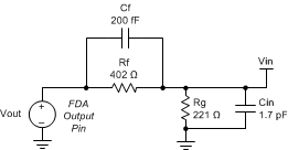 Figure 65. Feedback Network for the Gain of 2 Configuration Using 402 Ω and Matching to a 50-Ω Source
The response shape from Vout to Vin in Figure 65 has a pole and then a zero. To describe NG, invert the Laplace transform of Vin and Vout from Figure 65 to provide the frequency-dependent NG response of Equation 1, where a zero comes in first and then a pole.

The zero location is key. Using the gain of 2 values of Figure 65, the estimated zero in the NG is 588 MHz. Limiting the parasitic capacitance at the summing junctions, either differentially or signal-ended, to a ground or power plane is critical in board layouts.
Using this feedback model, and the open-loop gain and phase data for the THS4541-Q1, allows the Aol and NG curves over frequency to be drawn, as shown in Figure 66, where the peaking in the noise gain pulls the intersection point back in frequency.
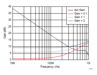 Figure 66. Aol and Noise Gain Plots for the Lower Gains of Figure 61
To assess closed-loop bandwidth and peaking, the noise-gain phase must be subtracted from the THS4541-Q1 Aol phase to obtain the total phase around the loop, as shown in Figure 67.
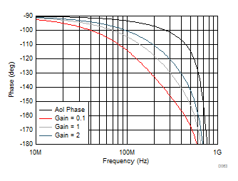 Figure 67. Loop-Gain Phase for the Three Lower Gains of Figure 1
From Figure 66 and Figure 67, using Table 2, tabulate the loop-gain crossover frequency and phase margin at these crossovers to explain the response shapes of Figure 1.
Table 2. Estimated Crossover Frequency and Phase Margin for Gains of 0.1, 1, and 2 in Figure 1
| GAIN | DC NG (V/V) | 0-dB LG (MHz) | PHASE MARGIN (°) |
|---|---|---|---|
| 0.1 | 1.1 | 457 | 18 |
| 1 | 1.94 | 380 | 41 |
| 2 | 2.85 | 302 | 59 |
From these crossover (or 0-dB loop gain) frequencies, a good approximation for the resulting f–3dB is to multiply the crossover frequencies by 1.6 when the phase margin is less than 65°. Ideally, a 65° phase margin at loop-gain crossover provides a flat Butterworth closed-loop response. The 59° phase margin for the gain of 2 setting explains the nearly flat response for this condition with 1.6 × 302 MHz = 483 MHz, estimated with f–3dB closely matching the measured 500-MHz SSBW.
The very low phase margin in the attenuator setting at 0.1 V/V explains the highly peaked response in Figure 1. This peaking can be easily compensated, as shown in the Designing Attenuators section, using feedback capacitors and a differential capacitor across the inputs.
Considering the noise gain zero as part of the loop-gain analysis shows the importance of using relatively-low, feedback-resistor values and minimizing layout parasitic capacitance on the input pins of the THS4541-Q1 to reduce the effects of this feedback pole. The TINA model does a good job of predicting these issues (the model includes the 0.85-pF differential internal capacitance); add any estimated external parasitic capacitance on the summing junctions in simulation to predict the response shape more accurately.
8.3 I/O Headroom Considerations
The starting point for most designs is usually to assign an output common-mode voltage. For AC-coupled signal paths, this voltage is often the default midsupply voltage, in order to retain the most available output swing around the centered Vocm. For DC-coupled designs, set this voltage with consideration for the required minimum headroom to the supplies shown in the specifications for the Vocm control. From the target output Vocm, the next step is to verify that the desired output differential VPP stays within the supplies. For any desired differential Vopp, check that the absolute maximum output pin swings with Equation 2 and Equation 3, and confirm they are within the supply rails for this rail-to-rail (RR) output device.


For instance, driving the ADC3223 with its 0.95 Vcm control using a single 3.3-V supply, the maximum output swing is set by the negative-going signal from 0.95 Vcm to +0.2 V above ground. This 0.75-V, single-sided swing becomes an available 4 × 0.75 V = 3 VPP differential around the nominal 0.95 Vcm output common mode. On the high side, the maximum output is 0.95 + 0.75 = 1.7 V. This result is well within the allowed maximum of 3.3 V – 0.2 V = 3.1 V. This 3 VPP is also well beyond the maximum required 2-VPP full-scale differential input for this ADC. However, having this extra swing range is useful if an interstage filter to the ADC adds insertion loss.
With the output headrooms confirmed, the input junctions must also stay within their operating range. The input range extends to the negative supply voltage (over the full temperature range); therefore, input range limitations usually appear only approaching the positive supply, where a maximum 1.3-V headroom is required over the full temperature range.
The input pins operate at voltages set by the external circuit design, the required output Vocm, and the input signal characteristics. For differential-to-differential designs where the input Vicm voltage does not move with the input signal, there are two configurations to consider:
- AC-coupled, differential-input designs have a Vicm equal to the output Vocm. The input Vicm requires approximately a 1.3-V headroom to the positive supply; therefore, the maximum Vocm to that value reduces from the Vocm positive headroom requirement of 1.2 V to the 1.3 V required on the input pins. The lower limit on the output Vocm is approximately 0.95 V to the negative supply over the full temperature range, and well within the 0-V minimum headroom on the input Vicm.
- DC-coupled, differential-input designs, check the voltage divider from the source Vcm to the THS4541-Q1 Vocm setting to confirm the resulting voltage divider solves to an input Vicm within the allowed range. If the source Vcm can vary over some voltage range, this result must be validated over that range.
For single-ended input to differential output designs, there is a DC Vicm voltage set by the external configuration with a small-signal related swing around that. The two conditions to consider are:
- AC-coupled, single-ended input to differential designs place an average input Vicm equal to the output Vocm voltage with an AC-coupled swing around that Vocm following the input voltage.
- DC-coupled, single-ended input to differential designs get a nominal input Vicm set by the source-signal common mode and the output Vocm setting with a small, signal-related swing around the DC Vicm level set by the voltage divider.
One method of deriving the voltage range for Vicm for any single-ended input to differential output design is to determine the voltage swing on the nonsignal-input side of the FDA outputs and simply take its divider back to the input pin to ground or the DC reference used on that side. An example analysis is shown in Figure 68, where the circuit of Figure 61 is simplified to show just a Thevenized source impedance.
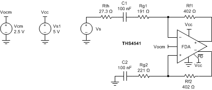 Figure 68. Input Swing Analysis Circuit from Figure 61 with Thevenized Source
For this AC-coupled input analysis, the nominal DC input Vicm is simply the output Vocm (2.5 V in this example design). Then, considering the lower side of the feedback networks, any desired maximum output differential VPP generates a known AC VPP at the junction of Rg2 and Rf2. For instance, if the design intends a maximum 4-VPP differential output, each FDA output pin is ±1 V around the Vocm (= 2.5 V), and then back to the Vicm, which produces a ±1 V × 221 / (221 + 402) = ±0.355 V around the DC setting of Vocm. This simple approach to assessing the input Vicm range for a single-ended to differential design can be applied to any design using an FDA by reducing the input side circuits to a divider to either the signal source and ground or voltage reference on the nonsignal input side.
8.4 Output DC Error and Drift Calculations and the Effect of Resistor Imbalances
The THS4541-Q1 offers a trimmed input offset voltage and extremely low offset drift over the full –40°C to +125°C operating range. This offset voltage combines with several other error contribution terms to produce an initial 25°C differential offset error band, and then a drift over temperature. For each error term, a gain must be assigned to that term. For this analysis, only DC-coupled signal paths are considered. One new source of output error (versus typical op amp analysis) arises from the effect that mismatched resistor values and ratios can have on the two sides of the FDA. Any common-mode voltage or drift creates a differential output error through the slight mismatches arising from the external feedback and gain-setting resistor tolerances, and the approximation (or snap) to standard value.
The error terms (25°C and drift), along with the gain to the output differential voltage, include:
- Input offset voltage—this voltage has a gain equal to the noise gain or 1 + Rf / Rg, where Rg is the total DC impedance from the input pins back to the source, or a DC reference (typically ground).
- Input offset current—this current has a gain to the differential output through the average feedback resistor value.
The remaining terms arise from an assumed range on both the absolute feedback resistor mismatch and the mismatch in the divider ratio on each side of the FDA. The first of these resistor mismatch terms is the input bias current creating a differential output offset because of Rf mismatch. For simplicity, the upper Rf and Rg values are called Rf1 and Rg1 with a ratio of Rf1 / Rg1 ≡ G1. The lower elements are defined as Rf2 and Rg2 with a ratio of Rf2 / Rg2 ≡ G2. To compute worst-case contributions, a maximum variation in the design resistor tolerance is used in the absolute and ratio mismatches. For instance, ±1% tolerance resistors are assumed, giving a worst-case G1 that is 2% higher than nominal and a G2 that is 2% lower than nominal, with a worst-case Rf value mismatch of 2% as well. For matched impedance designs with Rt and Rg1 on a single-ended to differential stage, the standard value snap imposes a fixed mismatch in the initial feedback ratios with the resistor tolerance adding a mismatch to this initial ratio mismatch. Define the selected external resistor tolerance as ±T (so for 1% tolerance resistors, T = 0.01).
- Total gain for bias current error is ±2 × T × Rfnom
Anything that generates an output common-mode level or shift over temperature also generates an output differential error term if the two feedback ratios, G1 and G2, are not equal. An error trying to produce a shift in the output common-mode is overridden by the common-mode control loop, where any feedback ratio mismatch creates a balanced, differential error around the Vocm output.
The terms that create a differential error from a common-mode term and feedback ratio mismatch include the desired Vocm voltage, any source common-mode voltage, any drift on the reference bias to the Vocm control pin, and any internal offset and drift in the Vocm control path.
Considering just the output common-mode control and the source common-mode voltage (Vicm), the conversion to output differential offsets is done by using Equation 4:

Neglecting any G1 and G2 mismatch because of standard values snap, the conversion gain for these two terms can be recast in terms of the nominal Rf / Rg ≡ G, and tolerance T, as shown in Equation 5. As G increases, this conversion gain approaches 4T, as a worst-case gain for these terms to output differential offset.

This conversion gain to differential output error is applied to two error terms: Vocm, assuming the input control pin is driven and not floating, and the source Vicm voltage. The source common-mode voltage is assumed to be 0 V in this example. If not, apply this gain to the source common-mode value or range in the intended application.
As a full example of using these terms to estimate the worst-case output 25°C error band, and then the worst-case drift (by adding all the error terms together independently), use the gain of 2 V/V configuration of Figure 63 with Rf = 402 Ω, and assume ±1% tolerance on the resistors with the standard values used in Figure 69.
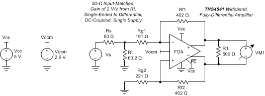 Figure 69. DC-Coupled Gain of 2 with Rf = 402 Ω and a Single-Ended to Differential Matched Input 50-Ω Impedance
The standard value snap on the signal-input side actually produces added G mismatch along with the resistor tolerances. For Figure 69, G2 = 402 / 221 = 1.819; and G1 = 402 / 218.3 = 1.837 nominally, with a ±2% tolerance around this initial mismatch for G2 and G1, if 1% resistors are used.
Using the maximum 25°C error terms, and a nominal 2.5-V input to the Vocm control pin, gives Table 3 with the error terms, the gains to the output differential error (Vod), and then the summed output error band at 25°C.
Table 3. Worst-Case Output Vod Error Band
| ERROR TERM | 25°C MAXIMUM VALUE | GAIN TO Vod | OUTPUT ERROR | |
|---|---|---|---|---|
| Input Vio | ±0.45 mV | 2.85 V/V | ±1.2825 mV | |
| Input Ios | ±0.5 µA | 402 Ω | ±0.201 mV | |
| Input Ibcm, Rf mismatch | 13 µA | ±8.04 Ω | ±0.105 mV | |
| Vocm input, G mismatch | 2.5 V | ±0.0322 | ±80.5 mV | |
| Total | ±82.09 mV | |||
The 0.03222 conversion gain for the G ratio mismatch is the worst case, starting from the initially higher G1 value because of standard value snap, and using a ±1% tolerance on the Rf and Rg elements of that ratio. The actual Vocm conversion gain range is not symmetric, but is shown that way here. The initial 25°C worst-case error band is dominated by the Vocm conversion to Vod through the feedback resistor ratio mismatch. Improve this G match and tolerances to reduce this term.
Normally, the expected drift in the output Vod is of more interest than an initial error band. Table 4 shows these terms and the summed results, adding all the terms independently to obtain a worst-case drift.
Table 4. Worst-Case Output Vod Drift Band
| ERROR TERM | DRIFT MAXIMUM VALUE | GAIN TO Vod | OUTPUT ERROR | |
|---|---|---|---|---|
| Input Vio | ±2.4 µV/°C | 2.85 V/V | ±6.84 µV/°C | |
| Input Ios | ±1.3 nA/°C | 402 Ω | ±0.522 µV/°C | |
| Input Ibcm, Rf mismatch | 15 nA/°C | ±8.04 Ω | ±0.121 µV/°C | |
| Vocm input, G mismatch | ±12 µV/°C | ±0.0322 | ±0.386 µV/°C | |
| Total | ±7.86 µV/°C | |||
In this calculation, the input offset voltage drift dominates the output differential offset drift. For the last term, the drift for the Vocm path is just for the internal offset drift of the common-mode path. Make sure to also consider the added external drift on the source of the Vocm input.
The absolute accuracy and drift for the THS4541-Q1 are exceptionally good. Mismatched resistor feedback ratios combined with a high drift in the Vocm control input can actually dominate the output Vod drift. Where the output differential precision is more important than the input matching accuracy, consider matching the networks on the two input sides to achieve improved nominal G1 to G2 match. The gains for the input bias current error terms are relatively low in this example design using 402-Ω feedback values. Higher Rf values give these terms more gain. A less conservative estimate of output drift considers the terms to be uncorrelated and RMS half of each terms worst-case span shown in Table 4. Performing this calculation for this example estimates a less conservative output offset drift of ±3.42 µV/°C; essentially, half the worst-case span of the input offset drift term. Follow these steps to estimate the output differential offset and drift for any external configuration.
8.5 Noise Analysis
The first step in the output noise analysis is to reduce the application circuit to its simplest form with equal feedback and gain setting elements to ground, as shown in Figure 70, with the FDA and resistor noise terms to be considered.
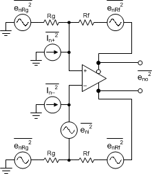 Figure 70. FDA Noise-Analysis Circuit
The noise powers are shown for each term. When the Rf and Rg terms are matched on each side, the total differential output noise is the RSS of these separate terms. Using NG ≡ 1 + Rf / Rg, the total output noise is given by Equation 6. Each resistor noise term is a 4kTR power.

The first term is simply the differential input spot noise times the noise gain. The second term is the input current noise terms times the feedback resistor (and because there are two terms, the power is two times one of the terms). The last term is the output noise resulting from both the Rf and Rg resistors, again times two, for the output noise power of each side added together. Using the exact values for a 50-Ω, matched, single-ended to differential gain, sweep with a fixed Rf = 402 Ω (see Table 6) and the intrinsic noise eni = 2.2 nV and In = 1.9 pA for the THS4541-Q1, gives an output spot noise from Equation 6. Then, dividing by the signal gain (Av) gives the input-referred, spot-noise voltage (ei) shown in Table 5.
Table 5. Swept Gain Output and Input-Referred, Spot-Noise Calculations(1)
| Av | Rt, EXACT (Ω) | Rg1, EXACT (Ω) | Rg2, EXACT (Ω) | NOISE GAIN | eno (nV/√Hz) | ei (nV/√Hz) |
|---|---|---|---|---|---|---|
| 1 | 55.2 | 399 | 425 | 1.94 | 6.64 | 6.64 |
| 2 | 60.1 | 191 | 218 | 2.85 | 8.71 | 4.36 |
| 3 | 65.6 | 124 | 153 | 3.63 | 10.7 | 3.56 |
| 4 | 72 | 89.7 | 119 | 4.37 | 12.1 | 3.03 |
| 5 | 79.7 | 67.8 | 98.3 | 5.09 | 13.7 | 2.74 |
| 6 | 89.1 | 54.2 | 86.5 | 5.65 | 15.4 | 2.56 |
| 7 | 101 | 43.2 | 76.6 | 6.25 | 16.7 | 2.39 |
| 8 | 117 | 35.2 | 70.1 | 6.74 | 17.3 | 2.16 |
| 9 | 138 | 29.0 | 65.8 | 7.11 | 18.6 | 2.06 |
| 10 | 170 | 23.6 | 62.5 | 7.44 | 18.9 | 1.89 |
| 11 | 220 | 18.7 | 59.3 | 7.78 | 19.6 | 1.78 |
| 12 | 313 | 14.6 | 57.7 | 7.97 | 20.0 | 1.66 |
| 13 | 545 | 10.8 | 56.6 | 8.11 | 20.3 | 1.56 |
| 14 | 2209 | 7.26 | 56.1 | 8.16 | 21.1 | 1.50 |
Notice that the input-referred ei is less than 2.2 nV/√Hz for just the THS4541-Q1 above a gain of 7 V/V. This result is because NG is less than Av when the source impedance is included in the NG calculation.
8.6 Factors Influencing Harmonic Distortion
As shown in the swept frequency harmonic distortion plots, the THS4541-Q1 provides extremely low distortion at lower frequencies. In general, FDA output harmonic distortion mainly relates to the open-loop linearity in the output stage corrected by the loop gain at the fundamental frequency. As the total load impedance decreases (including the effect of the feedback resistor elements in parallel for loading purposes), the output-stage, open-loop linearity degrades, increasing the harmonic distortion, as illustrated in Figure 16 and Figure 34. As the output voltage swings increase, very fine-scale, open-loop, output-stage nonlinearities increase, also degrading the harmonic distortion, as illustrated in Figure 14 and Figure 32. Conversely, decreasing the target output voltage swings drops the distortion terms rapidly. For harmonic-distortion testing, 2 VPP is used as a nominal swing because this value represents a typical ADC, full-scale, differential input range.
Increasing the gain acts to decrease the loop gain, resulting in the increasing harmonic distortion terms, as illustrated in Figure 18 and Figure 36. One advantage to the capacitive compensation for the attenuator design (described in the Designing Attenuators typical application example) is that the noise gain is shaped up with frequency to achieve a crossover at an acceptable phase margin at higher frequencies. This compensation holds the loop gain high at frequencies lower than the noise-gain zero, improving distortion in these lower bands.
Anything that moves the output pin voltage swings close to clipping into the supplies rapidly degrades harmonic distortion. Output clipping can occur from either absolute differential swing, or the swing can be moved closer to the supplies with the common-mode control. This effect is illustrated in Figure 17 and Figure 35.
The THS4541-Q1 does an exceptional job of converting from single-ended inputs to differential outputs with very low harmonic distortions. External resistors of 1% tolerance are used in characterization with good results. Imbalancing the feedback divider ratios does not degrade distortion directly. Imbalanced feedback ratios convert common-mode inputs to differential mode at the outputs with the gain described in the Output DC Error and Drift Calculations and the Effect of Resistor Imbalances section.
8.7 Driving Capacitive Loads
A very common requirement is driving the capacitive load of an ADC or some other next stage device. Directly driving a capacitive load with a closed-loop amplifier such as the THS4541-Q1 can lead to an unstable response, as shown in the step response plots into a capacitive load (see Figure 8 and Figure 26). One typical remedy for this instability is to add two small series resistors (Ro in Figure 71) at the outputs of the THS4541-Q1. Figure 6 and Figure 24 provide parametric plots of recommended Ro values versus differential capacitive load values and gain.
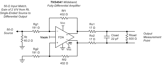 Figure 71. Including Ro when Driving Capacitive Loads
Operating at higher gains requires lower Ro values to achieve a ±0.5-dB flat response for the same capacitive load. Some direct parasitic loading is acceptable with no series Ro that increases with gain setting, as illustrated in Figure 6 and Figure 24 where the Ro value is 0 Ω. Even when these plots suggest no series Ro is required, good practice is to include a place for the Ro elements in the board layout (0-Ω load initially) for later adjustment, in case the response appears unacceptable. The TINA simulation model does a good job of predicting this effect and showing the impact for different choices of capacitive load isolating resistors (Ro).
8.8 Thermal Analysis
The relatively low internal quiescent power dissipation for the THS4541-Q1, combined with the excellent thermal impedance of the 16-pin VQFN (RGT) package, limits the possibility of excessively-high, internal-junction temperatures.
To estimate the internal junction temperature (TJ), an estimate of the maximum internal power dissipation (PD) is first required. There are two pieces to the internal power dissipation: quiescent current power and the power used in the output stage to deliver load current. To simplify the latter, the worst-case, output-stage power is driving a DC differential voltage across a load using half the total supply voltage. As an example:
- Assume a worst-case, 5% high 5-V supply. This 5.25-V supply with a maximum ICC of 11 mA gives a quiescent power term = 58 mW.
- Assume a 100-Ω differential load with a static 2.5-V differential voltage established across it. This 25 mA of DC load current generates a maximum output stage power of (5.25 V – 2.5 V) × 25 mA = 69 mW.
- From this total worst-case internal PD = 127 mW, multiply times the 52°C/W thermal impedance to get a 7°C rise from ambient.
Even for this extreme condition and the maximum rated ambient temperature of 125°C, the junction temperature is a maximum 132°C (less than the rated absolute maximum of 150°C). Follow this same calculation sequence for the exact application and package selected to predict the maximum TJ.