SNOSBH7F April 1999 – September 2014 LF412-N
PRODUCTION DATA.
6 Specifications
6.1 Absolute Maximum Ratings
over operating free-air temperature range (unless otherwise noted)(1)(8)| LF412A | LF412 | UNIT | ||||
|---|---|---|---|---|---|---|
| MIN | MAX | MIN | MAX | |||
| Supply Voltage | –22 | 22 | –18 | 18 | V | |
| Differential Input Voltage | –38 | 38 | –30 | 30 | V | |
| Input voltage Range(1) | ||||||
| Output Short Circuit Duration(2) | Continuous | Continuous | ||||
| TO Package | PDIP Package | |||||
| Power Dissipation(9) | See (3) | 670 | mW | |||
| Tj max | 150 | 115 | °C | |||
| Operating Temp. Range | See (4) | See (4) | ||||
| Lead Temp. (Soldering, 10 sec.) | 260 | 260 | °C | |||
(1) Stresses beyond those listed under Absolute Maximum Ratings may cause permanent damage to the device. These are stress ratings only, which do not imply functional operation of the device at these or any other conditions beyond those indicated under Recommended Operating Conditions. Exposure to absolute-maximum-rated conditions for extended periods may affect device reliability.
6.2 Handling Ratings
| TO and PDIP Package | UNIT | ||||
|---|---|---|---|---|---|
| MIN | MAX | ||||
| Tstg | Storage temperature range | −65 | 150 | °C | |
| V(ESD) | Electrostatic discharge | Human body model (HBM), per ANSI/ESDA/JEDEC JS-001, all pins(1) |
-1700 | 1700(10) | V |
| Charged device model (CDM), per JEDEC specification JESD22-C101, all pins(2) |
|||||
(1) JEDEC document JEP155 states that 500-V HBM allows safe manufacturing with a standard ESD control process.
(2) JEDEC document JEP157 states that 250-V CDM allows safe manufacturing with a standard ESD control process.
6.3 Recommended Operating Conditions
over operating free-air temperature range (unless otherwise noted)| MIN | NOM | MAX | UNIT | ||
|---|---|---|---|---|---|
| Supply Voltage LF412A | ±20 | V | |||
| Supply Voltage LF412 | ±15 | V | |||
6.4 Thermal Information
| THERMAL METRIC(1) | TO Package | PDIP Package | UNIT | |||
|---|---|---|---|---|---|---|
| RθJA | Junction-to-ambient thermal resistance (Typical) | 152 | 115 | °C/W | ||
| RθJC(top) | Junction-to-case (top) thermal resistance | |||||
| RθJB | Junction-to-board thermal resistance | |||||
| ψJT | Junction-to-top characterization parameter | |||||
| ψJB | Junction-to-board characterization parameter | |||||
| RθJC(bot) | Junction-to-case (bottom) thermal resistance | |||||
(1) For more information about traditional and new thermal metrics, see the IC Package Thermal Metrics application report, SPRA953.
6.5 DC Electrical Characteristics
over operating free-air temperature range (unless otherwise noted)| PARAMETER | TEST CONDITIONS | LF412A(5) | LF412(5) | UNIT | ||||||
|---|---|---|---|---|---|---|---|---|---|---|
| MIN | TYP | MAX | MIN | TYP | MAX | |||||
| VOS | Input Offset Voltage | RS=10 kΩ, TA=25°C | 0.5 | 1.0 | 1.0 | 3.0 | mV | |||
| ΔVOS/ΔT | Average TC of Input Offset Voltage | RS=10 kΩ | 7 | 7 | μV/°C | |||||
| IOS | Input Offset Current | VS=±15V(5)(6) | Tj=25°C | 25 | 100 | 25 | 100 | pA | ||
| Tj=70°C | 2 | 2 | nA | |||||||
| Tj=125°C | 25 | 25 | nA | |||||||
| IB | Input Bias Current | VS=±15V(5)(6) | Tj=25°C | 50 | 200 | 50 | 200 | pA | ||
| Tj=70°C | 4 | 4 | nA | |||||||
| Tj=125°C | 50 | 50 | nA | |||||||
| RIN | Input Resistance | Tj=25°C | 1012 | 1012 | Ω | |||||
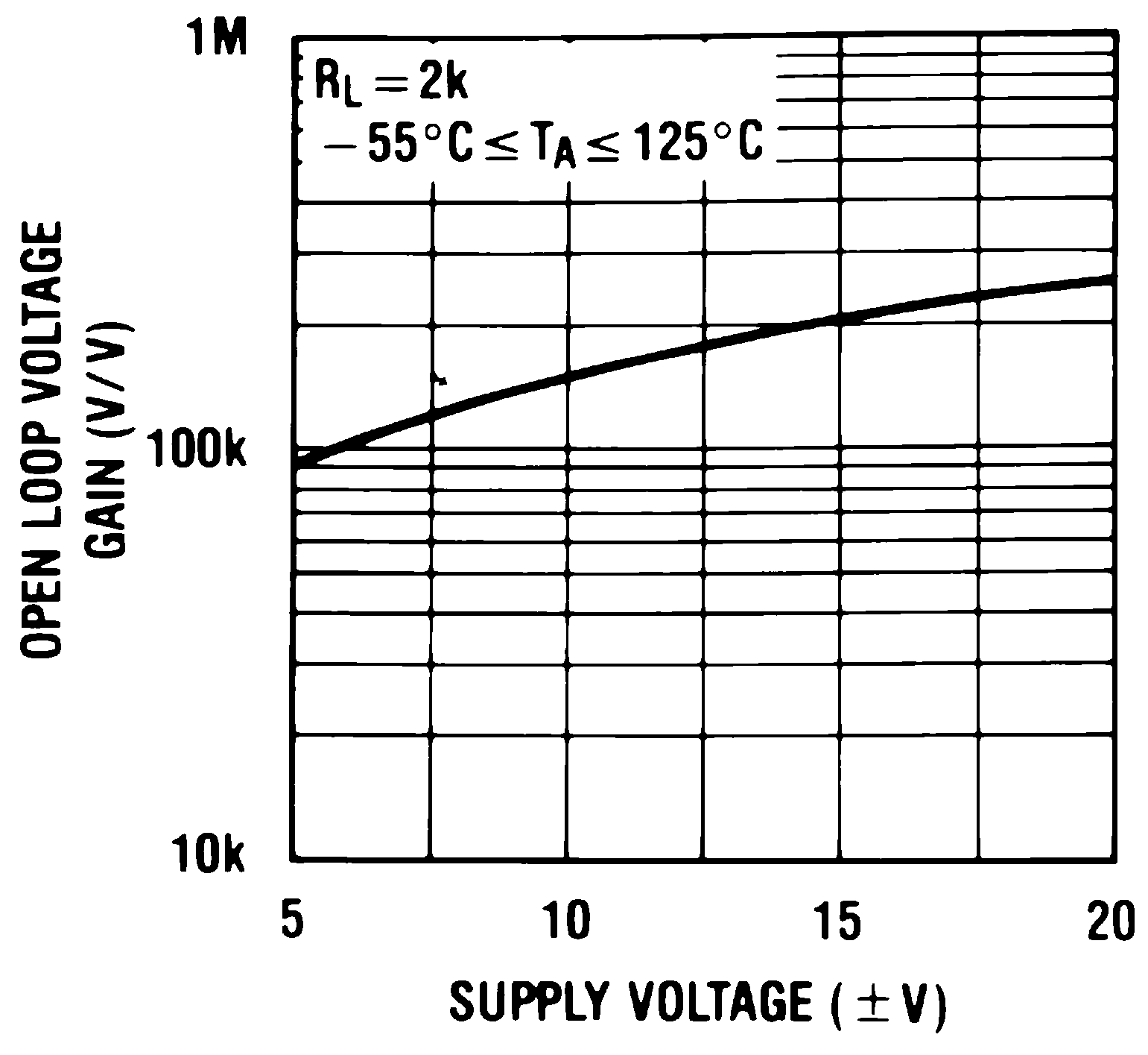
| AVOL | Large Signal Voltage Gain |
RL=2k, TA=25°C, VS=±15V, VO=±10V | 50 | 200 | 25 | 200 | V/mV | |||
| Over Temperature | 25 | 200 | 15 | 200 | ||||||
| VO | Output Voltage Swing | VS=±15V, RL=10k | ±12 | ±13.5 | ±12 | ±13.5 | V | |||
| VCM | Input Common-Mode Voltage Range | ±16 | +19.5 | ±11 | +14.5 | V | ||||
| −16.5 | −11.5 | V | ||||||||
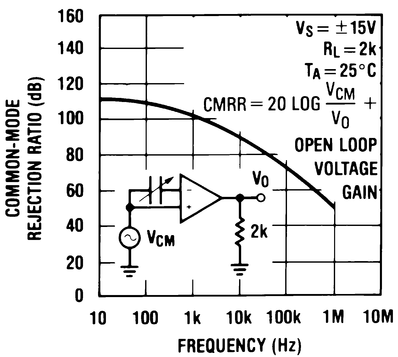
| CMRR | Common-Mode Rejection Ratio |
RS≤10k | 80 | 100 | 70 | 100 | dB | |||
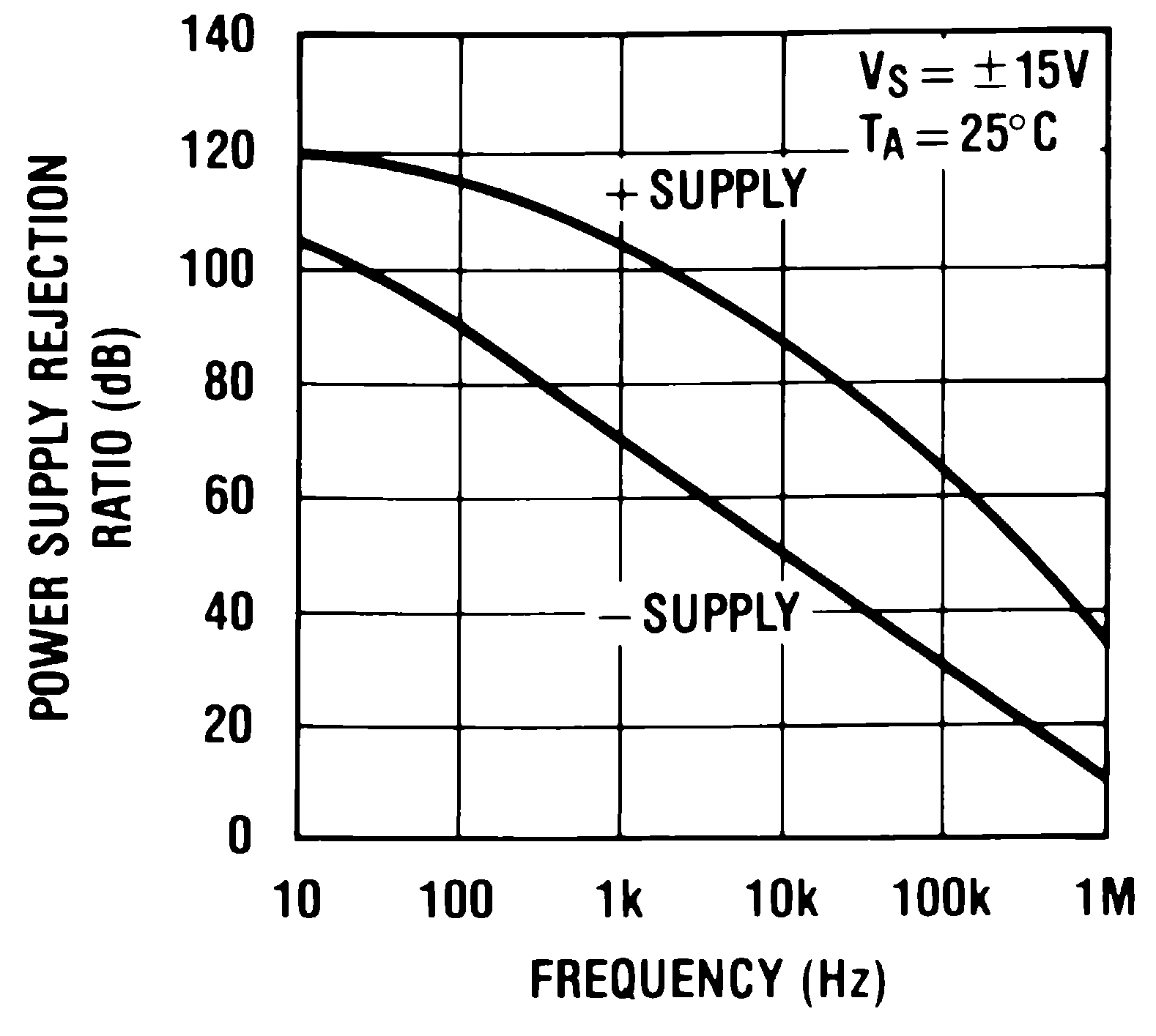
| PSRR | Supply Voltage Rejection Ratio |
See(7) | 80 | 100 | 70 | 100 | dB | |||
| IS | Supply Current | VO = 0V, RL = ∞ | 3.6 | 5.6 | 3.6 | 6.5 | mA | |||
6.6 AC Electrical Characteristics
over operating free-air temperature range (unless otherwise noted)| PARAMETER | TEST CONDITIONS | LF412A(5) | LF412(5) | UNIT | |||||
|---|---|---|---|---|---|---|---|---|---|
| MIN | TYP | MAX | MIN | TYP | MAX | ||||
| Amplifier to Amplifier Coupling |
TA=25°C, f=1 Hz-20 kHz (Input Referred) | −120 | −120 | dB | |||||
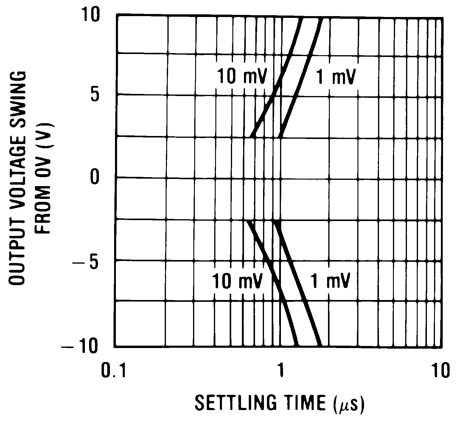
| SR | Slew Rate | VS=±15V, TA=25°C | 10 | 15 | 8 | 15 | V/μs | ||
| GBW | Gain-Bandwidth Product | VS=±15V, TA=25°C | 3 | 4 | 2.7 | 4 | MHz | ||
| THD | Total Harmonic Dist | AV=+10, RL=10k, VO=20 Vp-p, BW=20 Hz-20 kHz |
≤0.02% | ≤0.02% | |||||
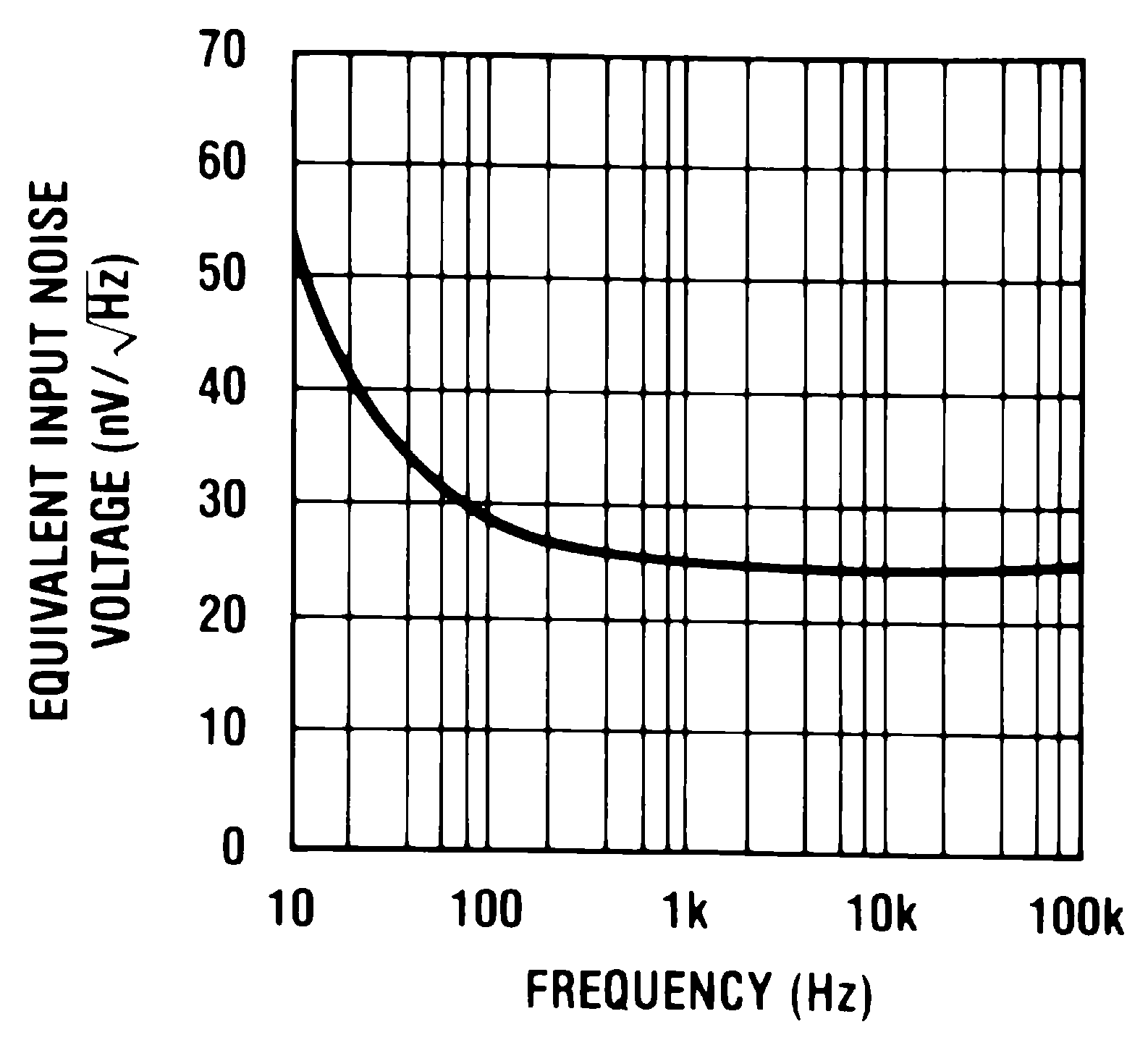
| en | Equivalent Input Noise Voltage |
TA=25°C, RS=100Ω, f=1 kHz |
25 | 25 | nV / √Hz | ||||
| in | Equivalent Input Noise Current |
TA=25°C, f=1 kHz | 0.01 | 0.01 | pA / √Hz | ||||
(1) Unless otherwise specified the absolute maximum negative input voltage is equal to the negative power supply voltage.
(2) Any of the amplifier outputs can be shorted to ground indefintely, however, more than one should not be simultaneously shorted as the maximum junction temperature will be exceeded.
(3) For operating at elevated temperature, these devices must be derated based on a thermal resistance of θjA.
(4) These devices are available in both the commercial temperature range 0°C≤TA≤70°C and the military temperature range −55°C≤TA≤125°C. The temperature range is designated by the position just before the package type in the device number. A “C” indicates the commercial temperature range and an “M” indicates the military temperature range. The military temperature range is available in TO package only. In all cases the maximum operating temperature is limited by internal junction temperature Tj max.
(5) Unless otherwise specified, the specifications apply over the full temperature range and for VS=±20V for the LF412A and for VS=±15V for the LF412. VOS, IB, and IOS are measured at VCM=0.
(6) The input bias currents are junction leakage currents which approximately double for every 10°C increase in the junction temperature, Tj. Due to limited production test time, the input bias currents measured are correlated to junction temperature. In normal operation the junction temperature rises above the ambient temperature as a result of internal power dissipation, PD. Tj=TA+θjA PD where θjA is the thermal resistance from junction to ambient. Use of a heat sink is recommended if input bias current is to be kept to a minimum.
(7) Supply voltage rejection ratio is measured for both supply magnitudes increasing or decreasing simultaneously in accordance with common practice. VS = ±6V to ±15V.
(8) Refer to RETS412X for LF412MH and LF412MJ military specifications.
(9) Max. Power Dissipation is defined by the package characteristics. Operating the part near the Max. Power Dissipation may cause the part to operate outside guaranteed limits.
(10) Human body model, 1.5 kΩ in series with 100 pF.
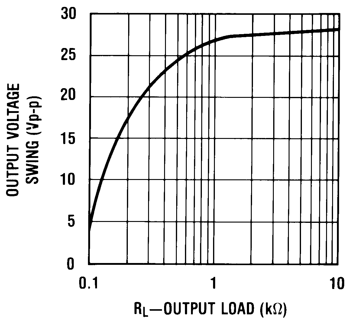
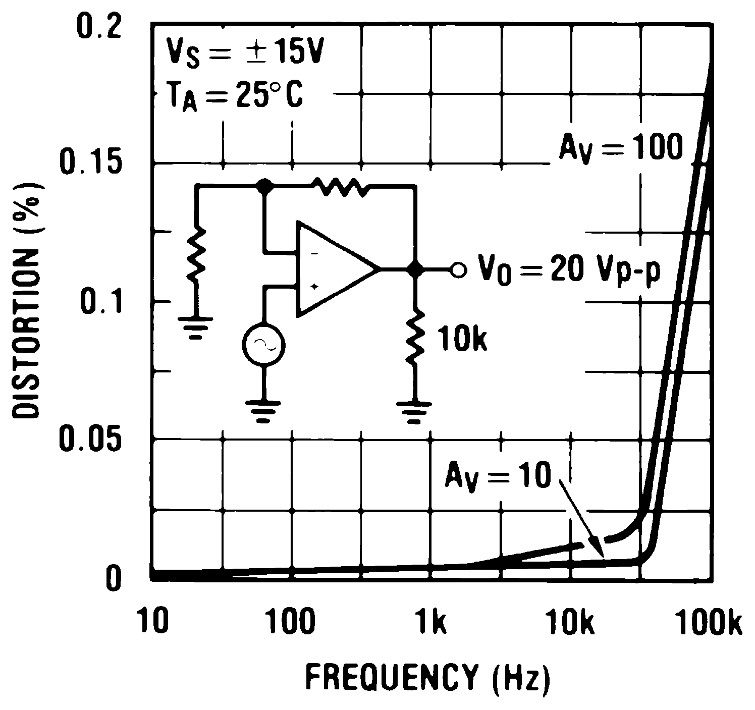
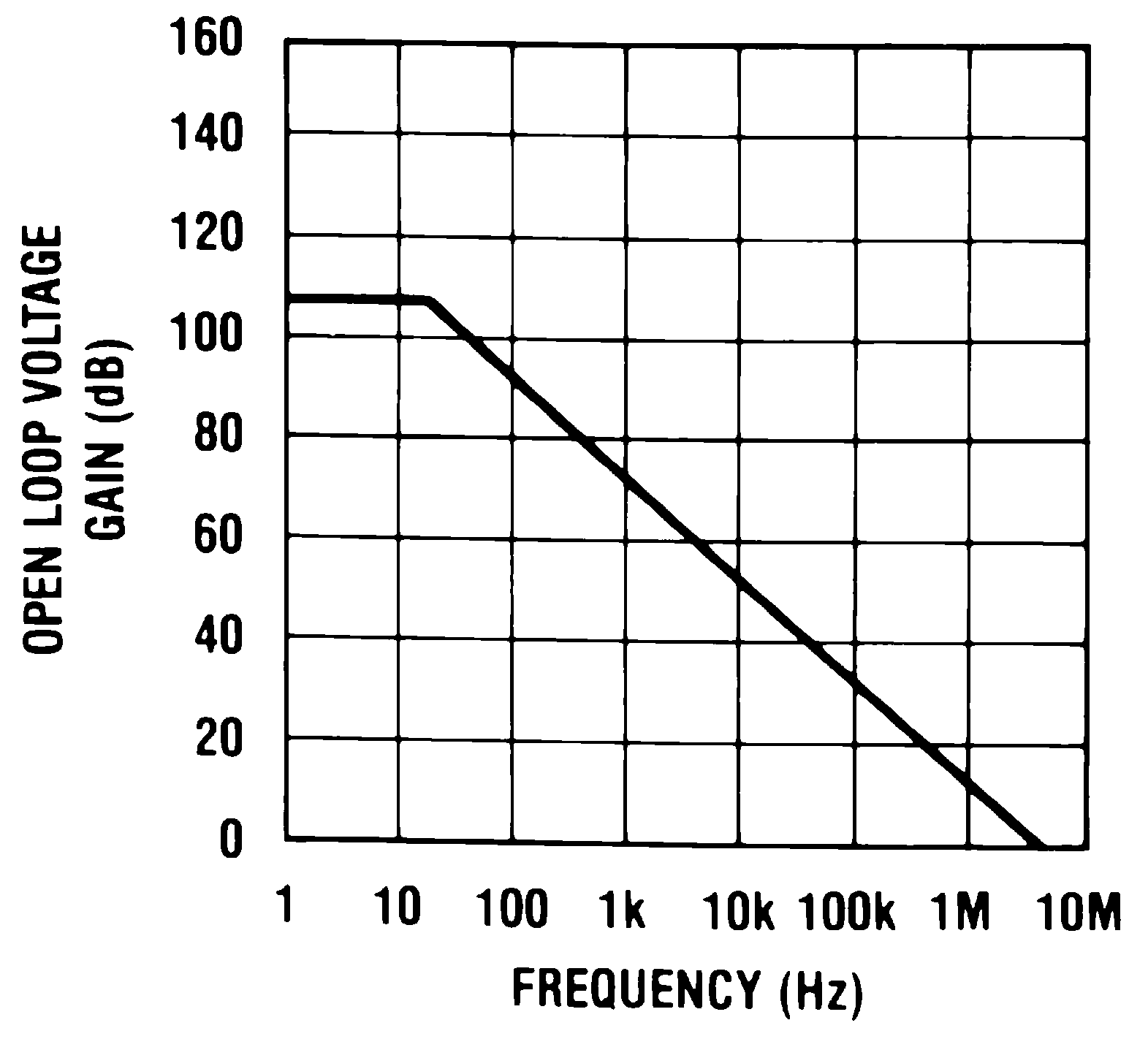
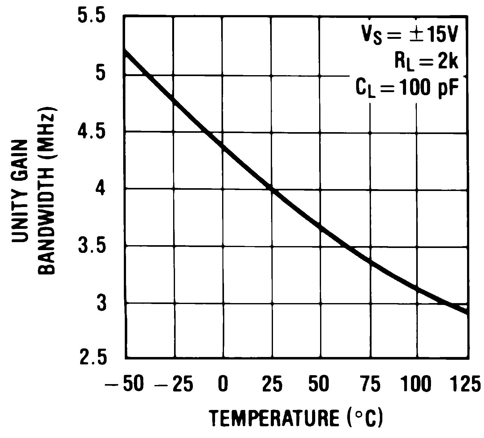
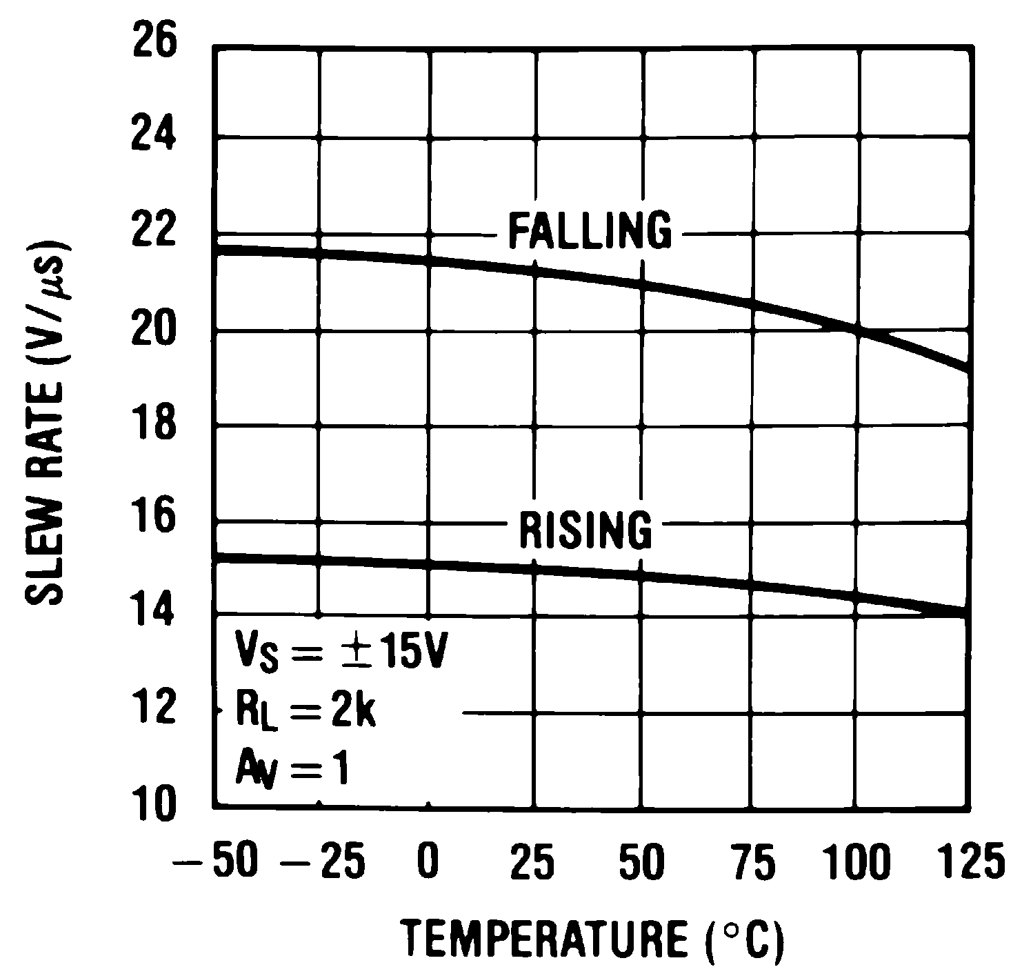
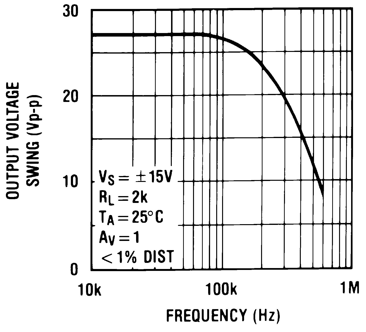
6.7 Typical Characteristics
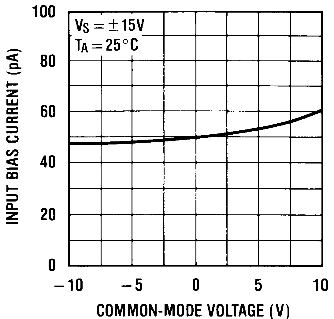
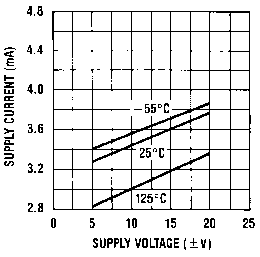
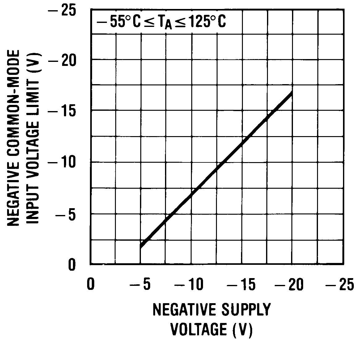 Figure 5. Negative Common-Mode
Input Voltage Limit
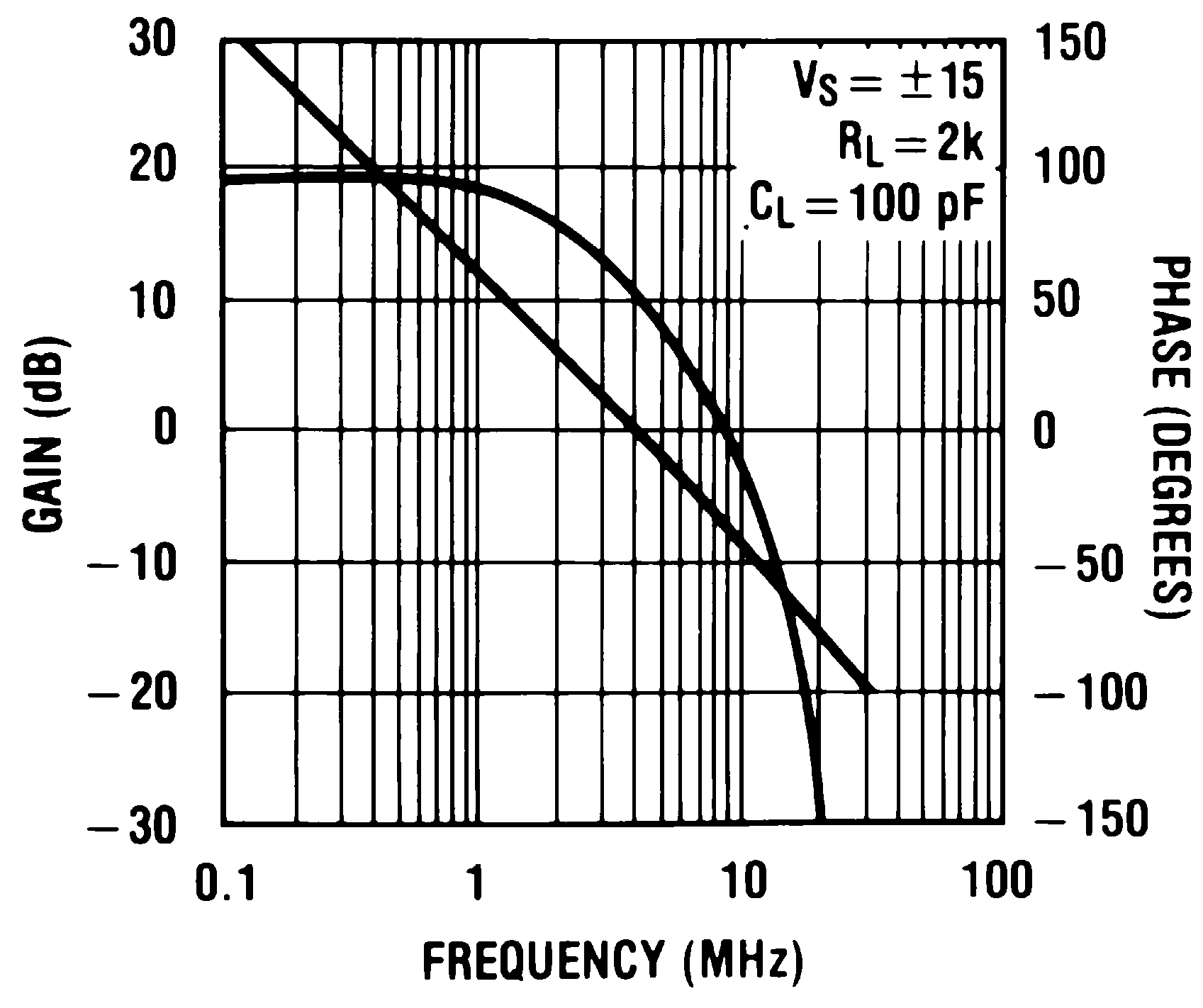
Frequency
Response
Ratio
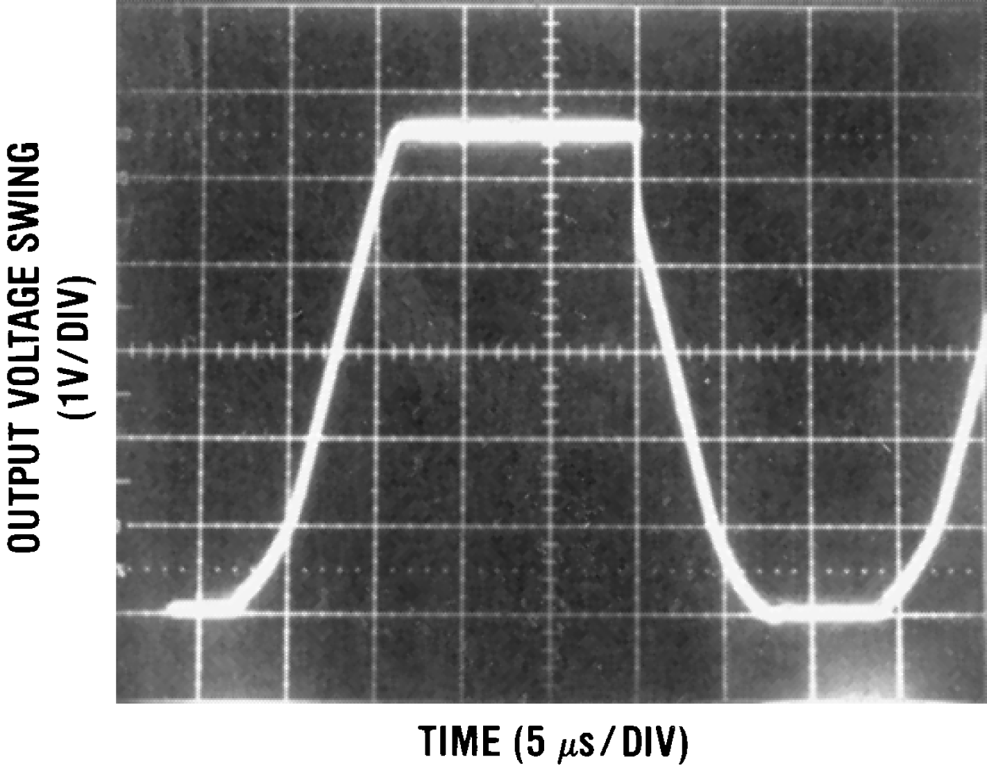
(RL = 2 kΩ, CL = 10 pF)
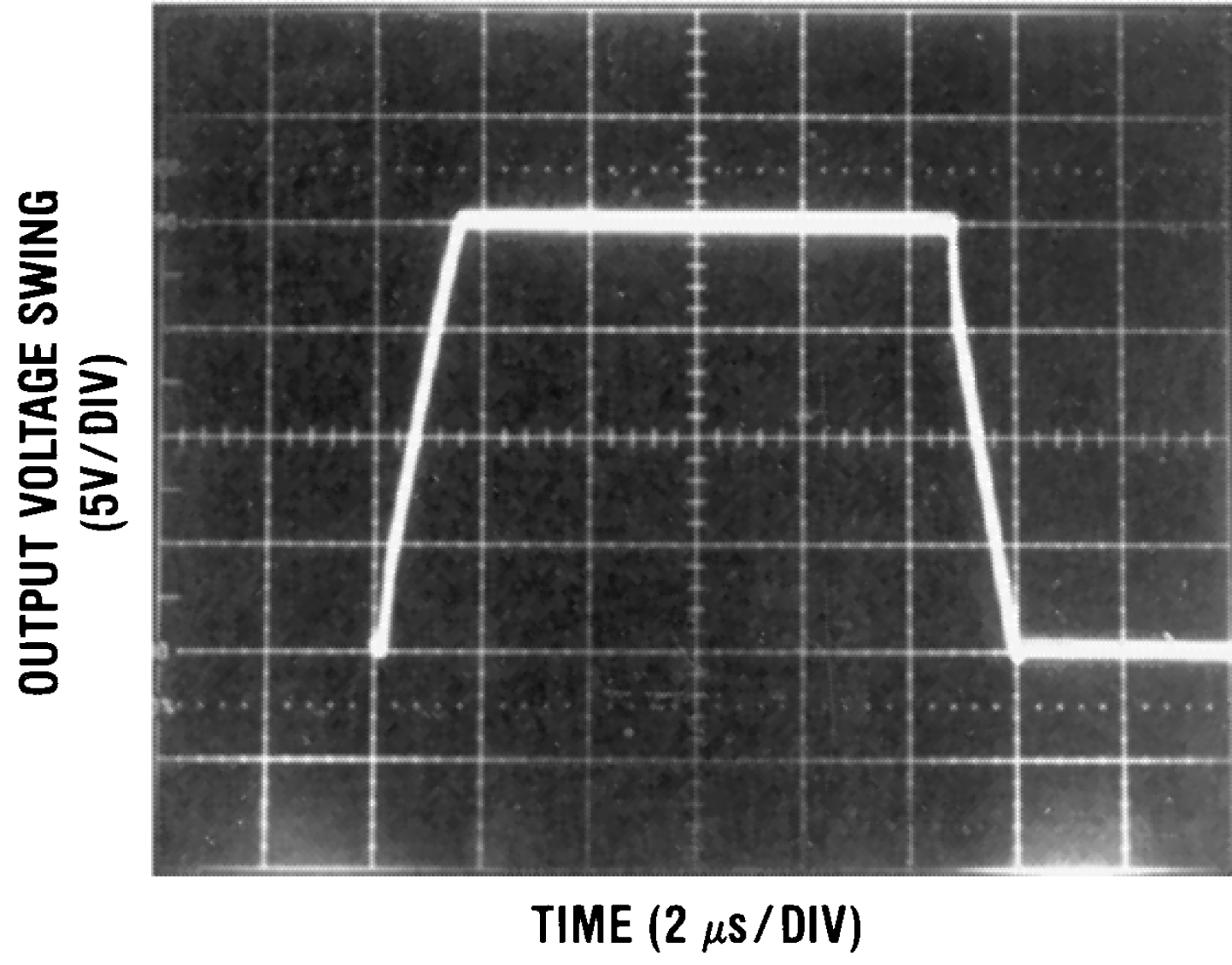
(RL = 2 kΩ, CL = 10 pF)
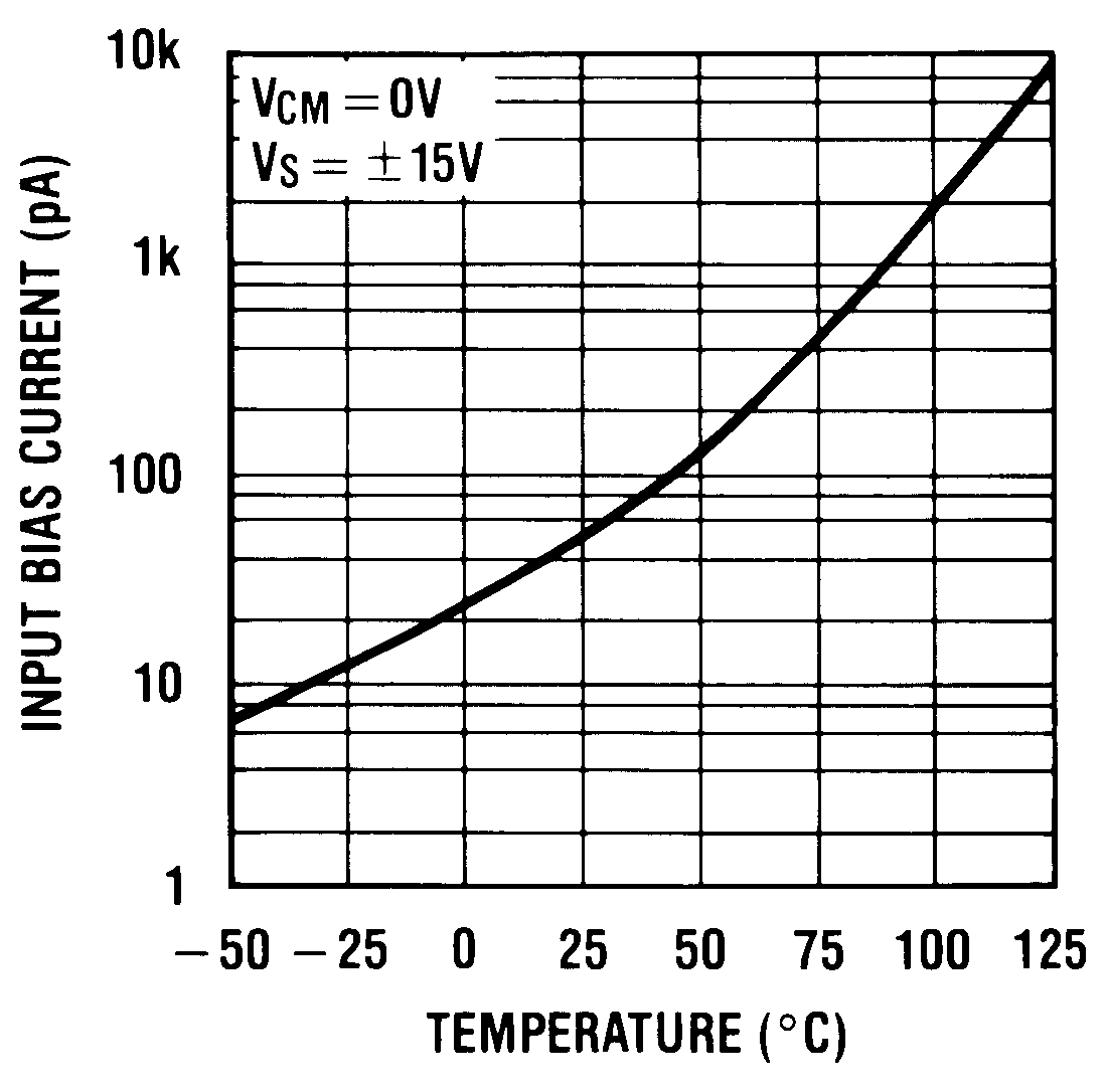 Figure 2. Input Bias Current
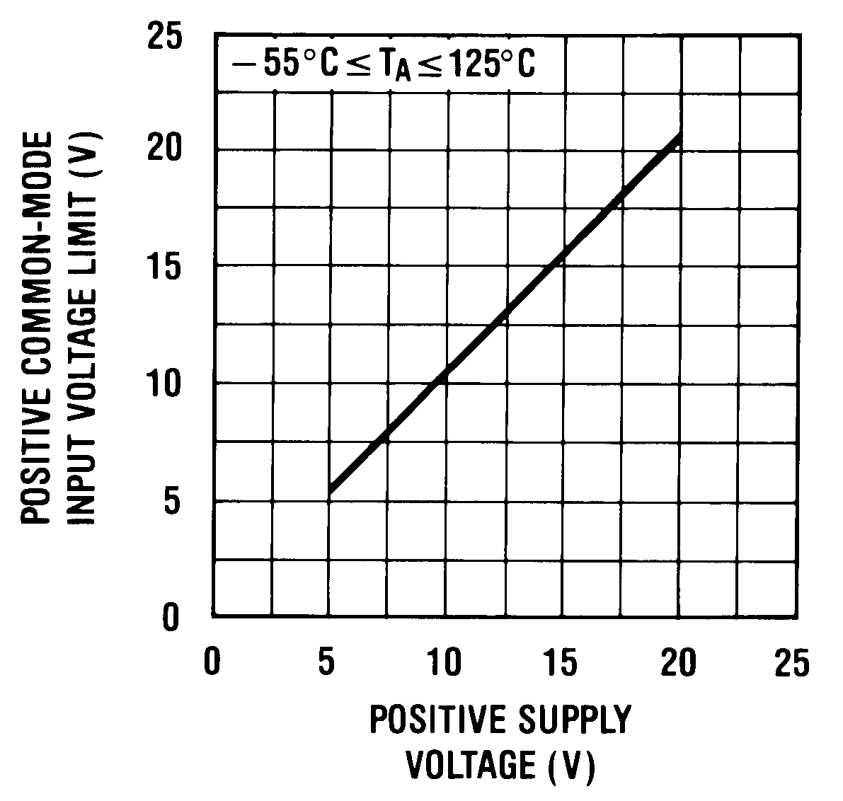 Figure 4. Positive Common-Mode
Input Voltage Limit
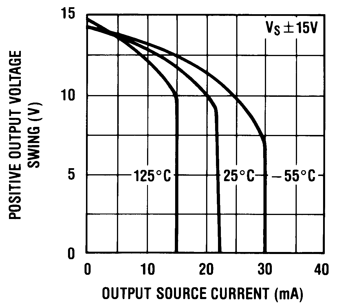
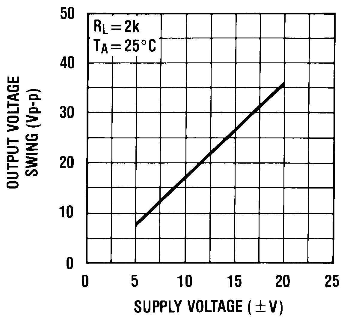
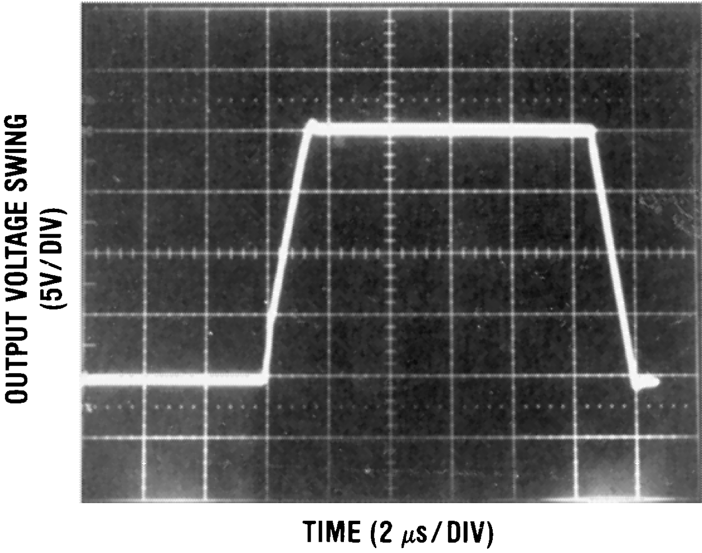
Swing
Ratio
Voltage
(RL = 2 kΩ, CL = 10 pF)
(RL = 2 kΩ, CL = 10 pF)
(CL = 10 pF)