ZHCSE92 September 2015 INA188
UNLESS OTHERWISE NOTED, this document contains PRODUCTION DATA.
8 Application and Implementation
NOTE
Information in the following applications sections is not part of the TI component specification, and TI does not warrant its accuracy or completeness. TI’s customers are responsible for determining suitability of components for their purposes. Customers should validate and test their design implementation to confirm system functionality.
8.1 Application Information
The INA188 measures a small differential voltage with a high common-mode voltage developed between the noninverting and inverting input. The low offset drift in conjunction with no 1/f noise makes the INA188 suitable for a wide range of applications. The ability to set the reference pin to adjust the functionality of the output signal offers additional flexibility that is practical for multiple configurations.
8.2 Typical Application
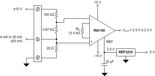
Figure 55 shows the basic connections required for operating the INA188. Applications with noisy or high-impedance power supplies may require decoupling capacitors close to the device pins. The output is referred to the output reference (REF) pin that is normally grounded. The reference pin must be a low-impedance connection to assure good common-mode rejection.
 Figure 55. PLC Input (±10 V, 4 mA to 20 mA)
8.2.1 Design Requirements
For this application, the design requirements are:
- 4-mA to 20-mA input with less than 20-Ω burden
- ±20-mA input with less than 20-Ω burden
- ±10-V input with impedance of approximately 100 kΩ
- Maximum 4-mA to 20-mA or ±20mA burden voltage equal to ±0.4 V
- Output range within 0 V to 5 V
8.2.2 Detailed Design Procedure
The following steps must be applied for proper device functionality:
- For a 4-mA to 20-mA input, the maximum burden of 0.4 V must have a burden resistor equal to 0.4 / 0.02 = 20 Ω.
- To center the output within the 0-V to 5-V range, VREF must equal 2.5 V.
- To keep the ±20-mA input linear within 0 V to 5 V, the gain resistor (RG) must be 12.4 kΩ.
- To keep the ±10-V input within the 0-V to 5-V range, attenuation must be greater than 0.05.
- A 100-kΩ resistor in series with a 4.87-kΩ resistor provides 0.0466 attenuation of ±10 V, well within the ±2.5-V linear limits.
8.2.3 Application Curve
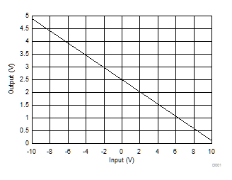
 Figure 56. Plot of PLC Input Transfer Function