ZHCSE92 September   2015 INA188

UNLESS OTHERWISE NOTED, this document contains PRODUCTION DATA.  

  1. 特性
  2. 应用范围
  3. 说明
  4. 修订历史记录
  5. Pin Configuration and Functions
  6. Specifications
    1. 6.1 Absolute Maximum Ratings
    2. 6.2 ESD Ratings
    3. 6.3 Recommended Operating Conditions
    4. 6.4 Thermal Information
    5. 6.5 Electrical Characteristics: VS = ±4 V to ±18 V (VS = 8 V to 36 V)
    6. 6.6 Electrical Characteristics: VS = ±2 V to < ±4 V (VS = 4 V to < 8 V)
    7. 6.7 Typical Characteristics
  7. Detailed Description
    1. 7.1 Overview
    2. 7.2 Functional Block Diagram
    3. 7.3 Feature Description
      1. 7.3.1 Inside the INA188
      2. 7.3.2 Setting the Gain
        1. 7.3.2.1 Gain Drift
      3. 7.3.3 Zero Drift Topology
        1. 7.3.3.1 Internal Offset Correction
        2. 7.3.3.2 Noise Performance
        3. 7.3.3.3 Input Bias Current Clock Feedthrough
      4. 7.3.4 EMI Rejection
      5. 7.3.5 Input Protection and Electrical Overstress
      6. 7.3.6 Input Common-Mode Range
    4. 7.4 Device Functional Modes
      1. 7.4.1 Single-Supply Operation
      2. 7.4.2 Offset Trimming
      3. 7.4.3 Input Bias Current Return Path
      4. 7.4.4 Driving the Reference Pin
      5. 7.4.5 Error Sources Example
  8. Application and Implementation
    1. 8.1 Application Information
    2. 8.2 Typical Application
      1. 8.2.1 Design Requirements
      2. 8.2.2 Detailed Design Procedure
      3. 8.2.3 Application Curve
  9. Power Supply Recommendations
  10. 10Layout
    1. 10.1 Layout Guidelines
    2. 10.2 Layout Example
  11. 11器件和文档支持
    1. 11.1 器件支持
      1. 11.1.1 开发支持
    2. 11.2 文档支持
      1. 11.2.1 相关文档 
    3. 11.3 社区资源
    4. 11.4 商标
    5. 11.5 静电放电警告
    6. 11.6 Glossary
  12. 12机械、封装和可订购信息

封装选项

机械数据 (封装 | 引脚)
散热焊盘机械数据 (封装 | 引脚)
订购信息

5 Pin Configuration and Functions

D Package
SOIC-8
Top View
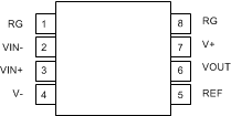
INA188 po_soic_sbos632.gif
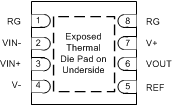
DRJ Package
WSON-8
Top View
INA188 po_drj_sbos632.gif

Pin Functions

PIN I/O DESCRIPTION
NO. NAME
REF 5 I Reference input. This pin must be driven by low impedance or connected to ground.
RG 1, 8 Gain setting pin. For gains greater than 1, place a gain resistor between pin 1 and pin 8.
V– 4 Negative supply
V+ 7 Positive supply
VIN– 2 I Negative input
VIN+ 3 I Positive input
VOUT 6 O Output