ZHCSE92 September 2015 INA188
UNLESS OTHERWISE NOTED, this document contains PRODUCTION DATA.
10 Layout
10.1 Layout Guidelines
Attention to good layout practices is always recommended. For best operational performance of the device, use good printed circuit board (PCB) layout practices, including:
- Care must be taken to ensure that both input paths are well-matched for source impedance and capacitance to avoid converting common-mode signals into differential signals. In addition, parasitic capacitance at the gain-setting pins can also affect CMRR over frequency. For example, in applications that implement gain switching using switches or PhotoMOS® relays to change the value of RG, select the component so that the switch capacitance is as small as possible.
- Noise can propagate into analog circuitry through the power pins of the circuit as a whole and of the device itself. Bypass capacitors are used to reduce the coupled noise by providing low-impedance power sources local to the analog circuitry.
- Connect low-ESR, 0.1-μF ceramic bypass capacitors between each supply pin and ground, placed as close to the device as possible. A single bypass capacitor from V+ to ground is applicable for single-supply applications.
- Separate grounding for analog and digital portions of the circuitry is one of the simplest and most effective methods of noise suppression. One or more layers on multilayer PCBs are usually devoted to ground planes. A ground plane helps distribute heat and reduces EMI noise pickup. Make sure to physically separate digital and analog grounds, paying attention to the flow of the ground current. For more detailed information, see SLOA089, Circuit Board Layout Techniques.
- In order to reduce parasitic coupling, run the input traces as far away from the supply or output traces as possible. If these traces cannot be kept separate, crossing the sensitive trace perpendicular is much better than in parallel with the noisy trace.
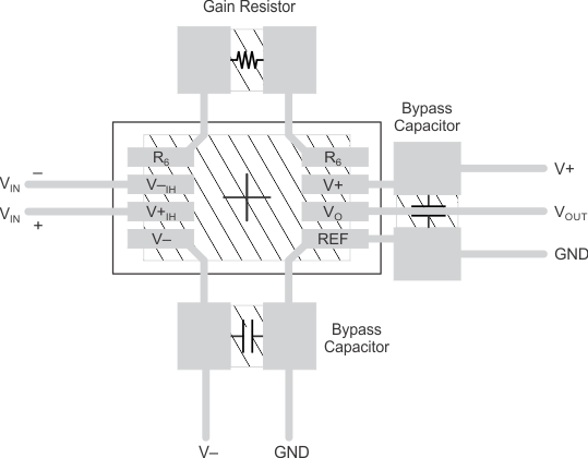
- Place the external components as close to the device as possible. As illustrated in Figure 57, keeping RG close to the pins minimizes parasitic capacitance.
- Keep the traces as short as possible.
10.2 Layout Example
 Figure 57. PCB Layout Example