SLUS395K February 2000 – October 2015 UCC2817 , UCC2818 , UCC3817 , UCC3818
PRODUCTION DATA.
- 1 Features
- 2 Applications
- 3 Description
- 4 Revision History
- 5 Pin Configuration and Functions
- 6 Specifications
- 7 Detailed Description
- 8 Application and Implementation
- 9 Power Supply Recommendations
- 10Layout
- 11Device and Documentation Support
- 12Mechanical, Packaging, and Orderable Information
封装选项
请参考 PDF 数据表获取器件具体的封装图。
机械数据 (封装 | 引脚)
- PW|16
- N|16
- DW|16
- D|16
散热焊盘机械数据 (封装 | 引脚)
订购信息
1 Features
- Controls Boost Preregulator to Near-Unity Power Factor
- Limits Line Distortion
- World Wide Line Operation
- Over-Voltage Protection
- Accurate Power Limiting
- Average Current Mode Control
- Improved Noise Immunity
- Improved Feed-Forward Line Regulation
- Leading Edge Modulation
- 150-μA Typical Start-Up Current
- Low-Power BiCMOS Operation
- Up to 18-V Operation
- Frequency Range 6 kHz to 220 kHz
2 Applications
- PC Power
- Consumer Electronics
- Lighting
- Industrial Power Supplies
- IEC6100-3-2 Compliant Supplies Less Than
300 W
3 Description
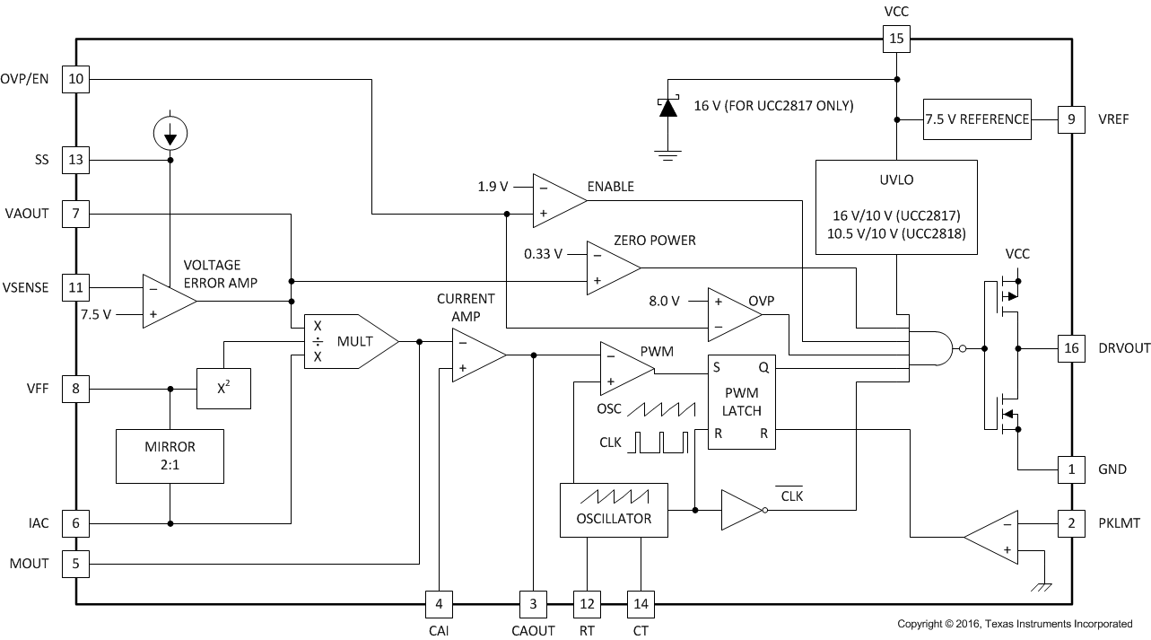
The UCCx817 and UCCx818 family provides all the functions necessary for active power factor-corrected preregulators. The controller achieves near-unity power factor by shaping the AC input line current waveform to correspond to that of the AC input line voltage. Average current mode control maintains stable, low distortion sinusoidal line current.
Designed in Texas Instrument’s BiCMOS process, the UCCx817 and UCCx818 offers new features such as lower start-up current, lower power dissipation, overvoltage protection, a shunt UVLO detect circuitry, a leading-edge modulation technique to reduce ripple current in the bulk capacitor, and an improved, low-offset (±2-mV) current amplifier to reduce distortion at light load conditions.
Device Information(1)
| PART NUMBER | PACKAGE | BODY SIZE (NOM) |
|---|---|---|
| UCC2817, UCC2818, UCC3817, UCC3818 | SOIC (16) | 3.91 mm × 9.9 mm |
| 7.5 mm × 10.3 mm | ||
| PDIP (16) | 6.35 mm × 19.3 mm |
- For all available packages, see the orderable addendum at the end of the data sheet.
Block Diagram
