SLUS395K February 2000 – October 2015 UCC2817 , UCC2818 , UCC3817 , UCC3818
PRODUCTION DATA.
- 1 Features
- 2 Applications
- 3 Description
- 4 Revision History
- 5 Pin Configuration and Functions
- 6 Specifications
- 7 Detailed Description
- 8 Application and Implementation
- 9 Power Supply Recommendations
- 10Layout
- 11Device and Documentation Support
- 12Mechanical, Packaging, and Orderable Information
封装选项
请参考 PDF 数据表获取器件具体的封装图。
机械数据 (封装 | 引脚)
- PW|16
- N|16
- DW|16
- D|16
散热焊盘机械数据 (封装 | 引脚)
订购信息
10 Layout
10.1 Layout Guidelines
10.1.1 Capacitor Ripple Reduction
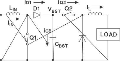
For a power system where the PFC boost converter is followed by a dc-to-dc converter stage, it can be beneficial to synchronize the two converters. In addition to the usual advantages such as noise reduction and stability, proper synchronization can significantly reduce the ripple currents in the output capacitor of the boost circuit. Figure 15 helps illustrate the impact of proper synchronization, by showing a PFC boost converter together with the simplified input stage of a forward converter.
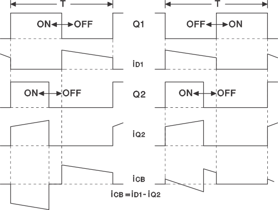
The capacitor current during a single switching cycle depends on the status of the switches Q1 and Q2, and is shown in Figure 16. With a synchronization scheme that maintains conventional trailing-edge modulation on both converters, the capacitor current ripple is highest. The greatest ripple current cancellation is attained when the overlap of Q1 offtime and Q2 ontime is maximized. One method of achieving this is to synchronize the turnon of the boost diode (D1) with the turnon of Q2. This approach implies that the leading edge of the boost converter is pulse-width modulated, while the forward converter is modulated with traditional trailing-edge PWM. The UCC3817 is designed as a leading-edge modulator with easy synchronization to the downstream converter to facilitate this advantage. Table 2 compares the ICB(rms) for D1/Q2 synchronization as offered by UCC3817 versus the ICB(rms) for the other extreme of synchronizing the turnon of Q1 and Q2 for a 200-W power system with a VBST of 385 V.
 Figure 15. Simplified Representation of a 2-Stage PFC Power Supply
 Figure 16. Timing Waveforms for Synchronization Scheme
Table 2. Effects of Synchronization on Boost Capacitor Current
| VIN = 85 V | VIN = 120 V | VIN = 240 V | ||||
|---|---|---|---|---|---|---|
| D(Q2) | Q1/Q2 | D1/Q2 | Q1/Q2 | D1/Q2 | Q1/Q2 | D1/Q2 |
| 0.35 | 1.491 A | 0.835 A | 1.341 A | 0.663 A | 1.024 A | 0.731 A |
| 0.45 | 1.432 A | 0.93 A | 1.276 A | 0.664 A | 0.897 A | 0.614 A |
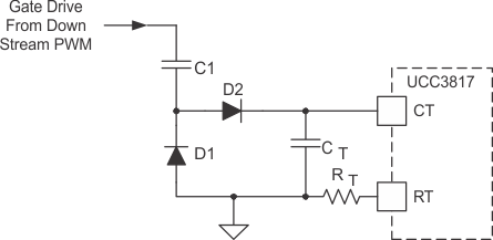
Table 2 illustrates that the boost capacitor ripple current can be reduced by approximately 50% at nominal line, and about 30% at high line with the synchronization scheme facilitated by the UCC3817. Figure 17 shows the suggested technique for synchronizing the UCC3817 to the downstream converter. With this technique, maximum ripple reduction as shown in Figure 16 is achievable. The output capacitance value can be significantly reduced if its choice is dictated by ripple current, or the capacitor life can be increased as a result. In cost-sensitive designs where holdup time is not critical, this is a significant advantage.
An alternative method of synchronization makes it possible to achieve the same ripple reduction. In this method, the turnon of Q1 is synchronized to the turnoff of Q2. While this method yields almost identical ripple reduction and maintains trailing edge modulation on both converters, the synchronization is more difficult to achieve, and the circuit can become susceptible to noise as the synchronizing edge itself is being modulated.
 Figure 17. Synchronizing the UCC3817 to a Down-Stream Converter
10.2 Layout Example
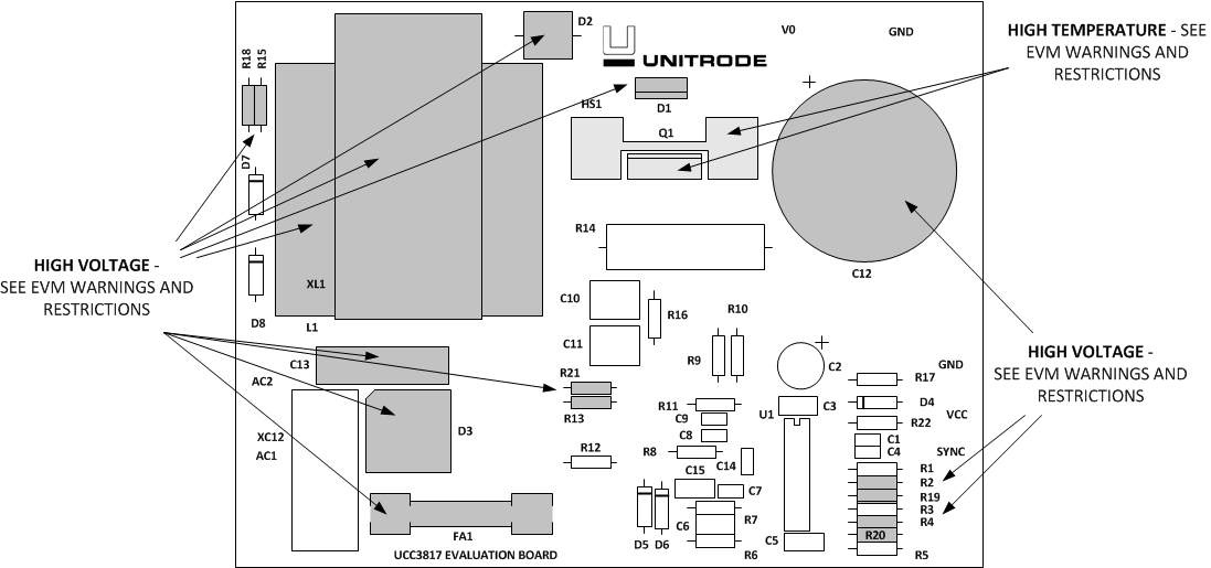
 Figure 18. UCC3817EVM Evaluation Board Layout Assembly