SNLS414E June 2012 – October 2016
PRODUCTION DATA.
- 1 Features
- 2 Applications
- 3 Description
- 4 Revision History
- 5 Pin Configuration and Functions
-
6 Specifications
- 6.1 Absolute Maximum Ratings
- 6.2 ESD Ratings
- 6.3 Recommended Operating Conditions
- 6.4 Thermal Information
- 6.5 Electrical Characteristics: DC
- 6.6 Switching Characteristics: AC
- 6.7 Timing Requirements: Serial Control Bus (CCI and I2C)
- 6.8 Timing Requirements: DC and AC Serial Control Bus (CCI and I2C)
- 6.9 Typical Characteristics
- 7 Detailed Description
- 8 Application and Implementation
- 9 Power Supply Recommendations
- 10Layout
- 11Device and Documentation Support
- 12Mechanical, Packaging, and Orderable Information
1 Features
- Automotive Grade Product: AEC-Q100 Grade 2 Qualified
- 10- to 75-MHz PCLK Support
(280-Mbps to 2.1-Gbps FPD-Link II Linerate) - Compatible to DC Balanced, AC-Coupled for FPD-Link II Serial Bit Stream
- Capable to Recover Data up to 10 Meters STP Cable
- MIPI D-PHY Modules Conform to v1.00.00
- Compatible With MIPI CSI-2 Version 1.01
- Supports Data Rate up to 900 Mbps per Data Lane With Two Lanes
- Video Stream Packet Formats: RGB888
- Continuous and Non-Continuous Clocking Mode
- Ultra Low Power, Escape, High Speed, and Control Modes Support
- Integrated Input Terminations and Adjustable Receive Equalization
- Fast Random Lock (No Reference Clock Required)
- CCI (Camera Control Interface) and I2C Compatible Control Bus
- @Speed BIST and Reporting Pin
- Single 1.8-V Power Supply
- 1.8-V or 3.3-V Compatible LVCMOS I/O Interface
- 8-kV ISO 10605 ESD Rating
- Leadless 40-Pin WQFN Package (6 mm × 6 mm)
2 Applications
- Automotive Infotainment:
- Central Information Displays
- Rear Seat Entertainment Systems
- Digital Instrument Clusters
3 Description
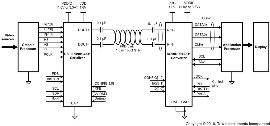
The DS90UR910-Q1 is an interface bridge chip that recovers data from the FPD-Link II serial bit stream and converts into a Camera Serial Interface (CSI-2) format compatible with Mobile Industry Processor Interface (MIPI) specifications. It recovers the 24- or 18-bit RGB data and 3 video sync-signals from the serial bit stream compatible to FPD-Link II serializers. The recovered data is packetized and serialized over two data lanes strobed by a half-rate serial clock compliant with the MIPI DPHY and CSI-2 specifications, each running up to 900 Mbps. The FPD-Link II receiver supports pixel clocks of up to
75 MHz. The CSI-2 output serial bus greatly reduces the interconnect and signal count to a graphic processing unit (GPU) and eases system designs for video streams from multiple automotive driver assist cameras.
The DS90UR910-Q1 is available in a 40-pin WQFN package. Electrical performance is qualified for automotive AEC-Q100 grade 2 temperature range
–40°C to 105°C.
Device Information(1)
| PART NUMBER | PACKAGE | BODY SIZE |
|---|---|---|
| DS90UR910-Q1 | WQFN (40) | 6.00 mm x 6.00 mm |
Applications Diagram
