SNLS414E June 2012 – October 2016
PRODUCTION DATA.
- 1 Features
- 2 Applications
- 3 Description
- 4 Revision History
- 5 Pin Configuration and Functions
-
6 Specifications
- 6.1 Absolute Maximum Ratings
- 6.2 ESD Ratings
- 6.3 Recommended Operating Conditions
- 6.4 Thermal Information
- 6.5 Electrical Characteristics: DC
- 6.6 Switching Characteristics: AC
- 6.7 Timing Requirements: Serial Control Bus (CCI and I2C)
- 6.8 Timing Requirements: DC and AC Serial Control Bus (CCI and I2C)
- 6.9 Typical Characteristics
- 7 Detailed Description
- 8 Application and Implementation
- 9 Power Supply Recommendations
- 10Layout
- 11Device and Documentation Support
- 12Mechanical, Packaging, and Orderable Information
7 Detailed Description
7.1 Overview
The DS90UR910-Q1 device recovers RBG data and sync signals from a FPD-Link II AC-coupled serial bit stream, and converts the recovered data into packetized CSI-2 data format. The CSI-2 output serial interface greatly reduces the interconnect and signal count to a graphic processing unit and eases system designs for video streams from multiple automotive driver assist cameras.
The DS90UR910-Q1 is based on the DS90UR906Q de-serializer core. See the DS90UR906Q data sheet, DS90UR90Q-Q1 5- to 65-MHz, 24-bit Color FPD-Link II Serializer and Deserializer (SNLS313), for the functionality and performance of the FPD-Link II interface can be found in the DS90UR906Q data sheet.
The DS90UR910-Q1 conforms to the MIPI CSI-2 and DPHY standards for protocol and electrical specifications. Compliant with standards:
- Conforms with MIPI Alliance Specification for D-PHY, version 1.00.00, dated May 14, 2009
- Compatible with MIPI Alliance Standard for Camera Serial Interface 2 (CSI-2) Version 1.01, dated Nov 9, 2010
The DS90UR910-Q1 receives 24-bit (or 18-bit) RGB data and 3 low speed control signals (VS, HS, DE) over a serial FPD-Link II transmitted through a single twisted pair. It supports a pixel clock of 10 MHz to 75 MHz, corresponding to the serial line rate of 280 Mb/s to 2100 Mb/s. The serial bit stream contains the scrambled 24-bit data, an embedded clock, encoded control signals and DC balance information which enhances signal quality and supports AC coupling.
The DS90UR910-Q1 is compatible with FPD-Link II serializers such as DS90UR905Q, DS90UR241Q, DS90C241Q, DS90UR907Q, DS99R421Q, and DS90Ux92x FPD-Link III serializers in backward compatibility mode. Figure 10 shows the serial bit stream. In each pixel clock cycle, a 28-bit frame is transmitted over the FPD-Link. The frame contains C1 and C0 representing the embedded clock information. C1 is always high and C0 is always low. Payload bits b[23:0] contain the scrambled 24-bit RGB data. DCB is the DC balance bit and is used to minimize the DC offset on the signal line. DCA is used to validate the data integrity in the embedded data stream and contain the encoded control signals VS, HS and DE (DS90UR905Q, DS90UR907Q, and DS90Ux92x in backward compatible mode).
 Figure 10. FPD-Link II Serial Stream
The DS90UR910-Q1 supports compatibility to FPD-Link II serializers and FPD-Link III serializers in backward compatible mode as defined in Table 1.
Table 1. DS90UR910-Q1 Configuration Modes
| CON FIG1 |
CON FIG0 |
MODE | FPD-LINK II COMPATIBILITY | CSI-2 DATA FORMAT |
|---|---|---|---|---|
| 0 | 0 | Normal mode, Control signal filter disabled | DS90UR905Q 24-bit, DS90UR907Q 24-bit, DS90Ux92x Serializers 24-bit |
RGB888 |
| 0 | 1 | Normal mode, Control signal filter enabled | DS90UR905Q 24-bit, DS90UR907Q 24-bit, DS90Ux92x Serializers 24-bit |
RGB888 |
| 1 | 0 | Backwards compatible GEN2 | DS90UR241Q 18-bit, DS99R421Q 18-bit |
RGB888 |
| 1 | 1 | Backwards compatible GEN1 | DS90C241Q 18-bit | RGB888 |
7.2 Functional Block Diagram
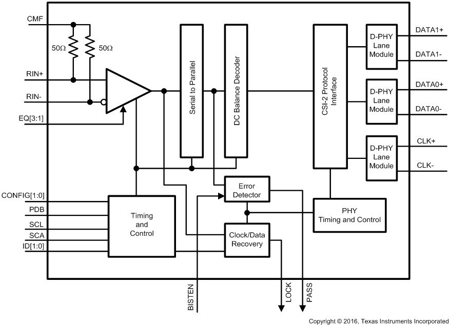
7.3 Feature Description
7.3.1 Input Receive Equalization
The input equalizer of the DS90UR910-Q1 is designed to compensate the attenuation distortion results from cable of different length or wire gauge. The equalizer gain setting is controlled by the control pins EQ[3:1] or through register programming. Users can optimize the equalizer’s gain setting along with the de-emphasis level of the DS90UR90xQ to achieve the optimum jitter performance.
Note this function cannot be seen at the RIN± input but can be observed at the serial test port (CMLOUT±) enabled through the serial bus control registers. The equalization feature may be controlled by the external pin or by register.
Table 2. Receiver Equalization Configuration
| INPUTS EQ[3:1] | EQ BOOST | ||
|---|---|---|---|
| EQ3 | EQ2 | EQ1 | |
| 0 | 0 | 1 | Approximately 3 dB |
| 0 | 1 | 0 | Approximately 4.5 dB |
| 0 | 1 | 1 | Approximately 6 dB |
| 1 | 0 | 0 | Approximately 7.5 dB |
| 1 | 0 | 1 | Approximately 9 dB |
| 1 | 1 | 0 | Approximately 10.5 dB |
| 1 | 1 | 1 | Approximately 12 dB |
| 0 | 0 | 0 | See(1) |
7.3.2 CSI-2 Interface
The DS90UR910-Q1 (in default mode) takes the RGB data bits R[7:0], G[7:0] and B[7:0] defined in the 24-bit serializer pinout and directly maps to the RGB888 color space in the data frame. The DS90UR910-Q1 follows the general frame format (see Figure 11). Upon the end of the vertical sync pulse (VS), the DS90UR910-Q1 generates the frame end and frame start synchronization packets within the vertical blanking period. The timing of the frame start does not reflect the timing of the VS signal.
Upon the rising edge of the DE signal, each active line is output in a long data packet with the RGB888 data format. At the end of each packet, the data lanes DATA0± and DATA1± return to the LP-11 state, while the clock lane CLK± continue outputting the high-speed clock.
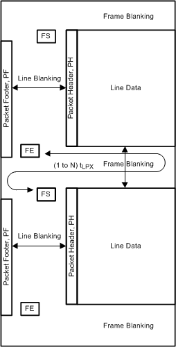 Figure 11. General Frame Format
7.3.3 High-Speed Clock and Data
The high-speed clock and data outputs are source synchronous interface. The half rate clock at CLK± is derived from the pixel clock sourced by the clock or data recovery circuit of the DS90UR910-Q1. The clock frequency is 6 times the pixel clock frequency. The 24-bit recovered RGB data is serialized and output at the 2 high-speed data lanes DATA0± and DATA1± in according to the CSI-2 protocol. The data rate of each lane is 12 times the pixel clock. As an example, at a pixel clock of 75 MHz, the CLK± runs at 450 MHz, and the data lanes run at
900 Mb/s.
The half-rate clock maintains a quadrature phase relationship to the data signals and allows receiver to sample data at the rising and falling edges of the clock. Figure 3 shows the timing relationship of the clock and data lines. The DS90UR910-Q1 supports continuous high-speed clock.
High-speed data are sent out at DATA0± and DATA1± in bursts. In between data bursts, the data lanes return to low power states in according to protocol defined in D-PHY standard. The rising edge of the differential clock (CLK+ – CLK–) is sent during the first payload bit of a transmission burst in the data lanes.
The DS90UR910-Q1 recovers the data bits R[7:0], G[7:0], B[7:0], VS, HS and DE from the serial FPD-Link II bit stream at RIN±. During the vertical blanking period (VS goes low), it sends the short frame end packet, followed by a short frame start packet. User can program the time between frame end to frame start packets from 0 to (216–1) in units of 8 × pclk_period / 3.
7.3.4 Data Frame RGB Mapping
Table 3 shows the pixel data R[7:0], G[7:0 and B[7:0] defined in DS90UR90xQ and DS90Ux92x serializers pinout, which are recovered by the DS90UR910-Q1 and output in RGB888 format (data type 0x24) at the CSI-2 interface.
Table 3. CSI-2 RGB888 Data Format With FPD-Link II Serializer (24-bit Mode)
| FPD-LINK II (24-BIT) PIN NAME |
RGB888 DATA BITS |
|---|---|
| R[0] | R[0] |
| R[1] | R[1] |
| R[2] | R[2] |
| R[3] | R[3] |
| R[4] | R[4] |
| R[5] | R[5] |
| R[6] | R[6] |
| R[7] | R[7] |
| G[0] | G[0] |
| G[1] | G[1] |
| G[2] | G[2] |
| G[3] | G[3] |
| G[4] | G[4] |
| G[5] | G[5] |
| G[6] | G[6] |
| G[7] | G[7] |
| B[0] | B[0] |
| B[1] | B[1] |
| B[2] | B[2] |
| B[3] | B[3] |
| B[4] | B[4] |
| B[5] | B[5] |
| B[6] | B[6] |
| B[7] | B[7] |
| HS | — |
| VS | — |
| DE | — |
 Figure 12. DATA0± and DATA1± Packet Format in According to CSI-2 Protocol for RGB888
Table 4. CSI-2 Data Format With FPD-Link II Serializers (18-Bit Mode)
| FPD-LINK II (18-BIT) PIN NAME |
RGB DATA BITS | CSI-2 RGB888 DATA BITS |
|---|---|---|
| — | — | R[0] |
| — | — | R[1] |
| DIN[0] | R[0] | R[2] |
| DIN[1] | R[1] | R[3] |
| DIN[2] | R[2] | R[4] |
| DIN[3] | R[3] | R[5] |
| DIN[4] | R[4] | R[6] |
| DIN[5] | R[5] | R[7] |
| — | — | G[0] |
| — | — | G[1] |
| DIN[6] | G[0] | G[2] |
| DIN[7] | G[1] | G[3] |
| DIN[8] | G[2] | G[4] |
| DIN[9] | G[3] | G[5] |
| DIN[10] | G[4] | G[6] |
| DIN[11] | G[5] | G[7] |
| — | — | B[0] |
| — | — | B[1] |
| DIN[12] | B[0] | B[2] |
| DIN[13] | B[1] | B[3] |
| DIN[14] | B[2] | B[4] |
| DIN[15] | B[3] | B[5] |
| DIN[16] | B[4] | B[6] |
| DIN[17] | B[5] | B[7] |
| DIN[18] | HS | — |
| DIN[19] | VS | — |
| DIN[20] | DE | — |
7.3.5 Display Timing Requirements
Table 5 shows the supported display resolutions for the DS90UR910-Q1. The display timings assume an estimated overall blanking rate of 1.2. The DS90UR910-Q1 automatically detects the incoming data rate by from the frame rate (by measuring VS). This timing is then mapped into a look up table. The lookup table is used for any pixel rate of PCLK from 10 MHz to 65 MHz. The limitation that it assumes the frame rate is 60 fps and
30 fps. An override option is available to set each of the parameter individually for a data rate that is not listed in the table. Option is programmed through CCI. Operation of frequencies above 65 MHz require additional I2C or CCI programming of CSI_TIMING registers.
Table 5. DS90UR910-Q1 Supported Resolution and Refresh Rates WITH Expected Blanking Period
| RESOLUTION | HACTIVE (PIXELS) | HBLANK (PIXELS) | HTOTAL (PIXELS) | VACTIVE (LINES) | VBLANK (LINES) | VTOTAL (LINES) | FRAME SIZE (PIXELS) | REFRESH (Hz) | PCLK (MHz) |
|---|---|---|---|---|---|---|---|---|---|
| 400 × 240 | 400 | 40 | 440 | 240 | 5 | 245 | 107800 | 60 | 6.468 |
| 640 × 240 | 640 | 40 | 680 | 240 | 5 | 245 | 166600 | 60 | 9.996 |
| 800 × 480 | 800 | 40 | 840 | 480 | 5 | 485 | 407400 | 60 | 24.444 |
| 1280 × 480 | 1280 | 40 | 1320 | 480 | 5 | 485 | 640200 | 60 | 38.412 |
| 640 × 480 | 640 | 144 | 784 | 480 | 29 | 509 | 399056 | 60 | 23.94336 |
| 800 × 600 | 800 | 256 | 1056 | 600 | 28 | 628 | 663168 | 60 | 39.79008 |
| 960 × 160 | 960 | 40 | 1000 | 160 | 5 | 165 | 165000 | 60 | 9.9 |
| 640 × 160 | 640 | 40 | 680 | 160 | 5 | 165 | 112200 | 60 | 6.732 |
| 480 × 240 | 480 | 96 | 576 | 240 | 24 | 264 | 152064 | 60 | 9.12384 |
| 800 × 480 | 800 | 160 | 960 | 480 | 48 | 528 | 506880 | 60 | 30.4128 |
| 1280 × 480 | 1280 | 256 | 1536 | 480 | 48 | 528 | 811008 | 60 | 48.66048 |
| 960 × 540 | 960 | 192 | 1152 | 540 | 54 | 594 | 684288 | 60 | 41.05728 |
| 1440 × 540 | 1440 | 288 | 1728 | 540 | 54 | 594 | 1026432 | 60 | 61.58592 |
| 1000 × 600 | 1000 | 200 | 1200 | 600 | 60 | 660 | 792000 | 60 | 47.52 |
| 640 × 480 | 640 | 160 | 800 | 480 | 45 | 525 | 420000 | 60 | 25.2 |
| 800 × 600 | 800 | 256 | 1056 | 600 | 28 | 628 | 663168 | 60 | 39.79008 |
| 1024 × 768 | 1024 | 320 | 1344 | 768 | 38 | 806 | 1083264 | 60 | 64.99584 |
| 1440 × 550 | 1440 | 144 | 1584 | 550 | 55 | 605 | 958320 | 60 | 57.4992 |
| 800 × 480 | 800 | 256 | 1056 | 480 | 45 | 525 | 554400 | 60 | 33.264 |
| 800 × 480 | 800 | 256 | 1056 | 480 | 45 | 525 | 554400 | 30 | 16.632 |
| 1024 × 480 | 1024 | 52 | 1076 | 480 | 24 | 504 | 542304 | 60 | 32.53824 |
| 1024 × 480 | 1024 | 52 | 1076 | 480 | 24 | 504 | 542304 | 30 | 16.26912 |
| 1024 × 480 | 1024 | 100 | 1124 | 480 | 48 | 528 | 593472 | 60 | 35.60832 |
| 1024 × 480 | 1024 | 100 | 1124 | 480 | 48 | 528 | 593472 | 30 | 17.80416 |
| 1440 × 550 | 1440 | 154 | 1594 | 550 | 55 | 605 | 964370 | 60 | 57.8622 |
| 1440 × 550 | 1440 | 154 | 1594 | 550 | 55 | 605 | 964370 | 30 | 28.9311 |
7.4 Device Functional Modes
7.4.1 Ultra-Low Power State
DS90UR910-Q1 D-PHY lanes enters ULPS mode upon software standby mode through Camera Control Interface (CCI) generated by application processor. When ULPS is entered, all lanes including the clock and data lanes are put in ULPS according to the MIPI D-PHY protocol. D-PHY can reduce power consumption by entering ULPS mode.
Ultra-low power state entry command is sent after an escape mode entry command through CCI, and then lane shall enter the Ultra-Low Power State (ULPS). When ULPS is entered, all lanes including the clock and data lanes are put in ULPS according to the MIPI DPHY protocol. Typically an ULPS entry command is used but other sequences can be used also. ULPS is exited by means of a mark-1 state with a length TWAKEUP followed by a stop state.
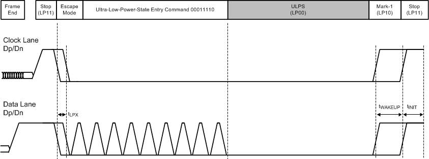 Figure 13. Ultra-Low Power State
7.4.2 Non-Continuous or Continuous Clock
DS90UR910-Q1 D-PHY supports continuous clock mode and non-continuous clock mode. Default mode is non-continuous clock mode, where the clock lane enters in LP mode between the transmissions of data packets. Non-continuous clock mode is only non-continuous during the vertical blanking period for lower PCLK rates. For higher PCLK rates, the clock is non-continuous between line and frame packets. Operating modes are configurable through CCI.
Clock lane enters LP11 during horizontal blanking if the horizontal blanking period is longer than the overhead time to start or stop the clock lane. There is auto-detection of the length of the horizontal blank period. The threshold is 70 PCLK cycles. Register bit available to disable off the non-continuous clock mode.
7.5 Programming
7.5.1 Serial Control Bus (CCI or I2C)
The DS90UR910-Q1 can be configured by the use of the CCI or I2C as defined by MIPI, which is a bi-directional, half-duplex, serial control bus consists of SCL and SDA. The SDA is the bi-directional data line. The SCL is the serial clock line. Both SCL and SDA are driven by open drain drivers and required external pullup resistors to VDDIO. The signals are either driven low or pulled high.
The DS90UR910-Q1 is a CCI slave. ID[1:0] pins select one of the four CCI slave addresses (see Table 6).
Table 6. CCI or I2C Slave Address
| ID[1] | ID[0] | 7-BIT SLAVE ADDRESS | 8-BIT SLAVE ADDRESS (0 APPENDED WRITE) |
|---|---|---|---|
| 0 | 0 | 011 1100 (0x3C’h) | 0111 1000 (0x78’h) |
| 0 | 1 | 011 1101 (0x3D’h) | 0111 1010 (0x7A’h) |
| 1 | 0 | 011 0110 (0x36’h) | 0110 1100 (0x6C’h) |
| 1 | 1 | 011 0111 (0x37’h) | 0110 1110 (0x6E’h) |
The serial bus protocol is initiated by START or START-REPEATED, and terminated by STOP condition. A START occurs when SDA transitions low while SCL is high. A STOP occurs when SDA transitions high when SCL is high (see Figure 14).
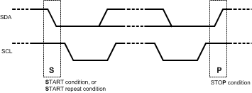 Figure 14. START and STOP Conditions
To communicate with a remote device, the host controller (master) sends the 7-bit slave address followed by a write-bit (0), and listens for a response from the slave. This response is referred to as an acknowledge bit. If the slave on the bus is addressed correctly, it acknowledges the master by driving the SDA low (ACK). If the address does not match the slave address of the device, it negative acknowledges the master by letting SDA be pulled high (NACK). In a write operation from master to slave, the master sends the 8-bit index address of the register that it wants to access. After the slave ACKs, the master sends the 8-bit data byte. The slave ACKs after each data byte is successfully received and is ready to receive another byte into the next sequential index location. At the end of the data transfer, the master ends the transaction with a STOP condition.
In a read operation, the master first sends the 8-bit index address of the register that it wants to access. After receiving an ACK from the slave, it initiates a START-REPEAT condition, sends the 7-bit slave address followed by the read-bit (1). The slave ACKs and sends out the 8-bit data byte. The master acknowledges an ACK when another data byte is sent to the next sequential index address. The master acknowledges an NACK when no more data byte is sent, and ends the transaction with a STOP condition.
The CCI interface of the DS90UR910-Q1 supports standard mode (<100 kHz) or fast mode (<400 kHz) with 8-bit index addressing and 8-bit data transfer. It supports the following read or write operations between the DS90UR910-Q1 and the CCI master:
- Single read from random location
- Single read from current location
- Sequential read starting from a random location
- Sequential read starting from the current location
- Single write to a random location
- Sequential write starting from a random location
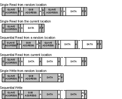 Figure 15. I2C or CCI Read or Write Operations
Table 7. Serial Bus Control Registers
| ADD (HEX) | REGISTER NAME | BIT(S) | R/W | DEFAULT | FIELD | DESCRIPTION |
|---|---|---|---|---|---|---|
| 0x00 | I2C_SLAVE_ID | 7:1 | R/W | 0x30 | DEVID | I2C slave ID |
| 0 | R/W | 0 | DEVID_EN | 0: Address from ID[X] Pin 1: Address from Register |
||
| 0x01 | CONFIG1 | 7 | R/W | 0 | LFMODE | If pin over write bit is one, controls the LF Mode. Debug only |
| 6 | R | 0 | Reserved | Reserved | ||
| 5 | R/W | 0 | SLEW | Control slew rate of LOCK, PASS and GPIO 0: Normal slew 1: Increased Slew |
||
| 4 | R | 0 | Reserved | Reserved | ||
| 3:2 | R/W | 0 | MODE | 00: Normal Mode, Control Signal Filter Disabled 01: Normal Mode, Control Signal Filter Enabled 10: Backwards Compatible (GEN2) 11: Backwards Compatible (GEN1) (See Table 1) |
||
| 1 | R/W | 0 | SLEEP | Note – not the same function as PowerDown (PDB pin) 0: Normal mode 1: Sleep Mode – Register settings retained. |
||
| 0 | R/W | 0 | USEREG | 0: Configurations set from control pins / STRAP pins 1: Override EQ and CONFIG strapped control inputs with register settings |
||
| 0x02 | CONFIG2 | 7:6 | R | 0 | Reserved | Reserved |
| 5:4 | R/W | 00 | OMAP | 6 bits to 8 bits color mapping 00: bit 4, 5 repeated on LSB 01: LSB zero if all data is zero 10: LSB zero 11: LSB zero |
||
| 3 | R | 0 | Reserved | Reserved | ||
| 2:0 | R/W | 3'b100 | Reserved | Reserved | ||
| 0x03 | EQ Control | 7:4 | R/W | 000 | EQ | Override EQ pin input if USEREG bit set |
| 3:0 | R | 0 | Reserved | Reserved | ||
| 0x04 | CMLOUT Config | 7 | R/W | 0 | CMLOUT | Loop through enable 0: Output CMLOUT± = disabled 1: Output CMLOUT± = enabled |
| 6:0 | R/W | 0 | VOD | VOD control 000000: min VOD 000001: 000011: 000111: 001111: 011111: 111111: max VOD |
||
| 0x05→0x10 | NA | 7:0 | R/W | 0 | Reserved | Reserved |
| 0x11 | CSI config | 7 | R/W | 0 | CCI_INV_VS | 0: VS is active low pulse 1: VS is active high pulse |
| 6 | R/W | 0 | CCI_CONT_CLOCK | 0: CSI-2 non-continuous clock 1: CSI-2 continuous clock |
||
| 5:2 | R/W | 0 | Reserved | Reserved | ||
| 1 | R/W | 0 | CCI_EXTERNAL_TIMING | 0: Use computed DPHY timing based on frame length 1: Use manual override values for DPHY timing |
||
| 0 | R/W | 0 | CCI_INV_DE | 0: DE is active low pulse 1: DE is active high pulse |
||
| 0x12 | CSI_FRM_GAP_0 | 7:0 | R/W | 0 | CSI_FRM_GAP_0 | Defined the delay between the start frame and end frame packet (lower byte) |
| 0x13 | CSI_FRM_GAP_1 | 7:0 | R/W | 0 | CSI_FRM_GAP_1 | Defined the delay between the start frame and end frame packet (upper byte) |
| 0x14 | CSI_TIMING0 | 7:5 | 0 | Reserved | Reserved | |
| 4:0 | R/W | 0 | TCLK_PREPARE | Defines the Tclk_prepare parameter if CCI_EXTERNAL_TIMING is set | ||
| 0x15 | CSI_TIMING1 | 7:3 | R/W | 0 | TCLK_ZERO | Defines the Tclk_zero parameter if CCI_EXTERNAL_TIMING is set |
| 2:0 | R/W | 0 | TCLK_TRAIL | Defines the Tclk_trail parameter if CCI_EXTERNAL_TIMING is set | ||
| 0x16 | CSI_TIMING2 | 7:4 | R/W | 0 | TCLK_POST | Defines the Tclk_post parameter if CCI_EXTERNAL_TIMING is set |
| 3:0 | R/W | 0 | THS_ZERO | Defines the Ths_zero parameter if CCI_EXTERNAL_TIMING is set | ||
| 0x17 | CSI_TIMING3 | 7 | R/W | 0 | Reserved | Reserved |
| 6:4 | R/W | 0 | THS_TRAIL | Defines the Ths_trail parameter if CCI_EXTERNAL_TIMING is set | ||
| 3:0 | R/W | 0 | THS_EXIT | Defines the Ths_exit parameter if CCI_EXTERNAL_TIMING is set | ||
| 0x18 | CSI_TIMING4 | 7:3 | R/W | 0 | THS_PREPARE | Defines the Ths_prepare parameter if CCI_EXTERNAL_TIMING is set |
| 2:0 | R/W | 0 | TLPX | Defines the Ths_exit parameter if CCI_EXTERNAL_TIMING is set | ||
| 0x19 | CSI_ULPS | 7:3 | R/W | 0 | Reserved | Reserved |
| 1 | R/W | 0 | ULPS_MODE | 0: In ULPS mode, data lane off 1: In ULPS mode, data lane off, clock lane off, x6 PLL off |
||
| 0 | R/W | 0 | ULPS_EN | 0: Disable UPLS mode 1: Enable ULPS mode |
||
| 0x1A | NA | 7:0 | R/W | 0 | Reserved | Reserved |
| 0x1B | CSI_UNH1 | 7 | R/W | 0 | Reserved | Reserved |
| 6:5 | R/W | 0x1 | ACT_VERT_MSB | MSBs of active vertical UNH image | ||
| 4:3 | R/W | 0x2 | TOT_VERT_MSB | MSBs of total vertical UNH image | ||
| 2:1 | R/W | 0 | Reserved | Reserved | ||
| 0 | R/W | 0 | PATGEN | 0: Normal mode 1: Enable pattern generator mode |
||
| 0x1C | CSI_UNH2 | 7:0 | R/W | 0x0F | TOT_VERT_LSB | LSBs of total vertical UNH image |
| 0x1D | CSI_UNH3 | 7:0 | R/W | 0xDF | ACT_VERT_LSB | LSBs of active vertical UNH image |
| 0x1E | CSI_UNH4 | 7:6 | R/W | 0 | Reserved | Reserved |
| 5:3 | R/W | 0x4 | ACT_HORIZ_MSB | MSBs of active horizontal UNH image | ||
| 2:0 | R/W | 0x5 | TOT_HORIZ_MSB | MSBs of total horizontal UNH image | ||
| 0x1F | CSI_UNH5 | 7:0 | R/W | 0xFF | ACT_HORIZ_LSB | LSBs of active horizontal UNH image |
| 0x20 | CSI_UNH6 | 7:0 | R/W | 0xFF | TOT_HORIZ_LSB | LSBs of total horizontal UNH image |
| 0x21 | CSI_UNH7 | 7:0 | R/W | 0x09 | PORCH_VERT | Vertical porch size UNH image |
| 0x22 | CSI_UNH8 | 7:0 | R/W | 0x09 | SYNC_VERT | Vertical sync size UNH image |
| 0x23 | CSI_UNH9 | 7:0 | R/W | 0x09 | PORCH_HORIZ | Horizontal porch size UNH image |
| 0x24→0x2F | NA | 7:0 | R/W | 0 | Reserved | Reserved |
| 0x30 | CSI_ID0 | 7:0 | R | 0x5F | CID0 | Chip ID, character _ |
| 0x31 | CSI_ID1 | 7:0 | R | 0x55 | CID1 | Chip ID, character U |
| 0x32 | CSI_ID2 | 7:0 | R | 0x52 | CID2 | Chip ID, character R |
| 0x33 | CSI_ID3 | 7:0 | R | 0x39 | CID3 | Chip ID, character 9 |
| 0x33 | CSI_ID4 | 7:0 | R | 0x31 | CID4 | Chip ID, character 1 |
| 0x35 | CSI_ID5 | 7:0 | R | 0x30 | CID5 | Chip ID, character 0 |
| 0x36 | CSI_REVID | 7:0 | R | 0x01 | CID5 | Revision ID of the design |
| 0x37→0x3A | NA | 7:0 | R | 0 | Reserved | Reserved |
| 0x3B | REVID | 7:0 | R | 0x01 | REVID | Revision ID of the design |
| 0x3C→0x3F | NA | 7:0 | R | 0 | Reserved | Reserved |
| 0x40→0xFF | Address range 0x00 to 0x3F aliases into the full address space. |