ZHCSHB7B September 2017 – July 2018 TPS7A53-Q1
PRODUCTION DATA.
- 1 特性
- 2 应用
- 3 说明
- 4 修订历史记录
- 5 Pin Configuration and Functions
- 6 Specifications
- 7 Detailed Description
-
8 Application and Implementation
- 8.1
Application Information
- 8.1.1 Recommended Capacitor Types
- 8.1.2 Soft Start and Inrush Current
- 8.1.3 Optimizing Noise and PSRR
- 8.1.4 Charge Pump Noise
- 8.1.5 Current Sharing
- 8.1.6 Adjustable Operation
- 8.1.7 Power-Good Operation
- 8.1.8 Undervoltage Lockout (UVLO) Operation
- 8.1.9 Dropout Voltage (VDO)
- 8.1.10 Device Behavior During Transition From Dropout Into Regulation
- 8.1.11 Load Transient Response
- 8.1.12 Reverse Current Protection Considerations
- 8.1.13 Power Dissipation (PD)
- 8.1.14 Estimating Junction Temperature
- 8.2 Typical Application
- 8.1
Application Information
- 9 Power Supply Recommendations
- 10Layout
- 11器件和文档支持
- 12机械、封装和可订购信息
7.3.1.1 DC Regulation
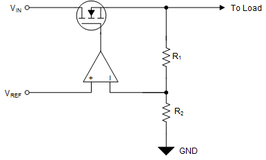
An LDO, as shown in Figure 39, functions as a class-B amplifier in which the input signal is the internal reference voltage (VREF). VREF is designed to have a very low bandwidth at the input to the error amplifier through the use of a low-pass filter (VNR/SS).
As such, the reference can be considered as a pure dc input signal. The low output impedance of an LDO comes from the combination of the output capacitor and pass element. The pass element also presents a high input impedance to the source voltage when operating as a current source. A positive LDO can only source current because of the class-B architecture.
This device achieves a maximum of 1% output voltage accuracy primarily because of the high-precision band-gap voltage (VBG) that creates VREF. The low dropout voltage (VDO) reduces the thermal power dissipation required by the device to regulate the output voltage at a given current level, thereby improving system efficiency. These features combine to make this device a good approximation of an ideal voltage source.

NOTE:
VOUT = VREF × (1 + R1 / R2).