-
ISO782xLL 高性能 8000 VPK 增强型隔离式双 LVDS 缓冲器
- 1 特性
- 2 应用
- 3 说明
- 4 修订历史记录
- 5 Pin Configuration and Functions
-
6 Specifications
- 6.1 Absolute Maximum Ratings
- 6.2 ESD Ratings
- 6.3 Recommended Operating Conditions
- 6.4 Thermal Information
- 6.5 Power Ratings
- 6.6 Insulation Specifications
- 6.7 Safety-Related Certifications
- 6.8 Safety Limiting Values
- 6.9 DC Electrical Characteristics
- 6.10 DC Supply Current Characteristics
- 6.11 Switching Characteristics
- 6.12 Insulation Characteristics Curves
- 6.13 Typical Characteristics
- 7 Parameter Measurement Information
- 8 Detailed Description
- 9 Application and Implementation
- 10Power Supply Recommendations
- 11Layout
- 12器件和文档支持
- 13机械、封装和可订购信息
- 重要声明
ISO782xLL 高性能 8000 VPK 增强型隔离式双 LVDS 缓冲器
1 特性
- 符合 TIA/EIA-644-A LVDS 标准
- 信号传输速率:高达 100Mbps
- 宽电源电压范围:2.25V 至 5.5V
- 宽环境温度范围:-55°C 至 +125°C
- 低功耗,100Mbps 时每通道的电流:
- 典型值 9.3mA (ISO7820LL)
- 典型值 9.5mA (ISO7821LL)
- 低传播延迟:17ns(典型值)
- 行业领先的 CMTI(最小值):±100kV/μs
- 优异的电磁兼容性 (EMC)
- 系统级静电放电 (ESD)、瞬态放电 (EFT) 以及抗浪涌保护
- 低辐射
- 隔离栅寿命:> 40 年
- 提供宽体和超宽体 SOIC-16 封装
- 可承受的隔离浪涌电压高达 12800 VPK
- 安全相关认证:
- 符合 DIN V VDE V 0884-10 (VDE V 0884-10):2006-12 标准的 8000 VPK
- 符合 UL 1577 标准且长达 1 分钟的 5700 VRMS 隔离
- CSA 组件验收通知 5A,IEC 60950-1 和 IEC 60601-1 终端设备标准
- 符合 EN 61010-1 和 EN 60950-1 标准的 TUV 认证
- GB4943.1-2011 CQC 认证
- 已通过所有认证
2 应用
- 电机控制
- 测试和测量
- 工业自动化
- 医疗设备
- 通信系统
3 说明
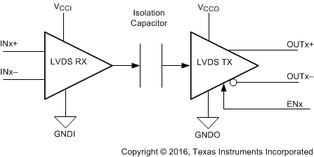
ISO782xLL 系列器件是高性能隔离式双路 LVDS 缓冲器,隔离电压高达 8000VPK。在隔离 LVDS 总线信号时,该器件可提供高电磁抗扰度,辐射较低,并且具有低功耗特性。每条隔离通道的 LVDS 接收和发送缓冲器均由二氧化硅 (SiO2) 绝缘栅相隔离。
ISO7820LL 器件有两个正向通道。ISO7821LL 器件有一条正向通道和一条反向通道。
凭借创新型芯片设计和布线技术,ISO782xLL系列器件的电磁兼容性得到了显著增强,可缓解系统级 ESD、EFT 和浪涌问题并符合辐射标准。
ISO782xLL 系列器件提供 16 引脚 SOIC 宽体 (DW) 和超宽体 (DWW) 两种封装。
器件信息(1)
| 器件型号 | 封装 | 封装尺寸(标称值) |
|---|---|---|
| ISO7820LL ISO7821LL |
DW (16) | 10.30mm x 7.50mm |
| DWW (16) | 10.30mm x 14.00mm |
- 要了解所有可用封装,请见数据表末尾的可订购产品附录。
简化电路原理图
5 Pin Configuration and Functions
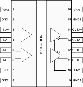
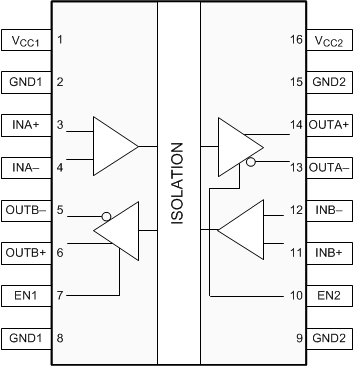
Pin Functions
| PIN | I/O | DESCRIPTION | ||
|---|---|---|---|---|
| NAME | NO. | |||
| ISO7820LL | ISO7821LL | |||
| EN1 | — | 7 | I | Output enable 1. Output pins on side 1 are enabled when EN1 is high or open and in high impedance state when EN1 is low. |
| EN2 | 10 | 10 | I | Output enable 2. Output pins on side 2 are enabled when EN2 is high or open and in high impedance state when EN2 is low. |
| GND1 | 2 | 2 | — | Ground connection for VCC1 |
| 8 | 8 | |||
| GND2 | 9 | 9 | — | Ground connection for VCC2 |
| 15 | 15 | |||
| INA+ | 3 | 3 | I | Positive differential input, channel A |
| INA– | 4 | 4 | I | Negative differential input, channel A |
| INB+ | 6 | 11 | I | Positive differential input, channel B |
| INB– | 5 | 12 | I | Negative differential input, channel B |
| NC | 7 | — | — | Not connected |
| OUTA+ | 14 | 14 | O | Positive differential output, channel A |
| OUTA– | 13 | 13 | O | Negative differential output, channel A |
| OUTB+ | 11 | 6 | O | Positive differential output, channel B |
| OUTB– | 12 | 5 | O | Negative differential output, channel B |
| VCC1 | 1 | 1 | — | Power supply, side 1, VCC1 |
| VCC2 | 16 | 16 | — | Power supply, side 2, VCC2 |
6 Specifications
6.1 Absolute Maximum Ratings
over operating free-air temperature range (unless otherwise noted)(1)| MIN | MAX | UNIT | |||
|---|---|---|---|---|---|
| VCCx | Supply voltage(2) | VCC1, VCC2 | –0.5 | 6 | V |
| V | Voltage on input, output, and enable pins | OUTx, INx, ENx | –0.5 | VCCx + 0.5(3) | V |
| IO | Maximum current through OUTx pins | –20 | 20 | mA | |
| TJ | Junction temperature | –55 | 150 | °C | |
| Tstg | Storage temperature | –65 | 150 | °C | |
6.2 ESD Ratings
| VALUE | UNIT | |||
|---|---|---|---|---|
| V(ESD) | Electrostatic discharge | Human-body model (HBM), per ANSI/ESDA/JEDEC JS-001(1) | ±4500 | V |
| Charged-device model (CDM), per JEDEC specification JESD22-C101(2) | ±1500 | |||
6.3 Recommended Operating Conditions
| MIN | NOM | MAX | UNIT | |||
|---|---|---|---|---|---|---|
| VCC1, VCC2 | Supply voltage | 2.25 | 3.3 | 5.5 | V | |
| |VID| | Magnitude of RX input differential voltage | Driven with voltage sources on RX pins | 100 | 600 | mV | |
| VIC | RX input common-mode voltage | VCC1, VCC2 ≥ 3 V | 0.5 |VID| | 2.4 – 0.5 |VID| | V | |
| VCC1, VCC2 < 3 V | 0.5 |VID| | VCCx – 0.6 – 0.5 |VID| | V | |||
| RL | TX far end differential termination | 100 | Ω | |||
| DR | Signaling rate | 0 | 100 | Mbps | ||
| TA | Ambient temperature | –55 | 25 | 125 | °C | |
6.4 Thermal Information
| THERMAL METRIC(1) | ISO7820LL ISO7821LL |
UNIT | |||
|---|---|---|---|---|---|
| DW (SOIC) | DWW (SOIC) | ||||
| 16 PINS | 16 PINS | ||||
| RθJA | Junction-to-ambient thermal resistance | 82 | 84.6 | °C/W | |
| RθJC(top) | Junction-to-case(top) thermal resistance | 44.6 | 46.4 | °C/W | |
| RθJB | Junction-to-board thermal resistance | 46.6 | 55.3 | °C/W | |
| ψJT | Junction-to-top characterization parameter | 17.8 | 18.7 | °C/W | |
| ψJB | Junction-to-board characterization parameter | 46.1 | 54.5 | °C/W | |
| RθJC(bottom) | Junction-to-case(bottom) thermal resistance | — | — | °C/W | |
6.5 Power Ratings
VCC1 = VCC2 = 5.5 V, TJ = 150°C, CL = 5 pF, input a 50-MHz 50% duty-cycle square wave, EN1 = EN2 = 5.5 V,RL = 100-Ω differential
| PARAMETER | TEST CONDITIONS | MIN | TYP | MAX | UNIT | |
|---|---|---|---|---|---|---|
| ISO7821LL | ||||||
| PD | Maximum power dissipation (both sides) | 156 | mW | |||
| PD1 | Maximum power dissipation (side 1) | 78 | mW | |||
| PD2 | Maximum power dissipation (side 2) | 78 | mW | |||
| ISO7820LL | ||||||
| PD | Maximum power dissipation (both sides) | 152 | mW | |||
| PD1 | Maximum power dissipation (side 1) | 36 | mW | |||
| PD2 | Maximum power dissipation (side 2) | 116 | mW | |||
6.6 Insulation Specifications
over operating free-air temperature range (unless otherwise noted)(1)| PARAMETER | TEST CONDITIONS | SPECIFICATION | UNIT | ||
|---|---|---|---|---|---|
| DW | DWW | ||||
| GENERAL | |||||
| CLR | External clearance(1) | Shortest terminal-to-terminal distance through air | >8 | >14.5 | mm |
| CPG | External creepage(1) | Shortest terminal-to-terminal distance across the package surface | >8 | >14.5 | mm |
| DTI | Distance through the insulation | Minimum internal gap (internal clearance) | >21 | >21 | μm |
| CTI | Tracking resistance (comparative tracking index) | DIN EN 60112 (VDE 0303–11); IEC 60112; UL 746A | >600 | >600 | V |
| Material group | According to IEC 60664-1 | I | I | ||
| Overvoltage category per IEC 60664-1 | Rated mains voltage ≤ 600 VRMS | I–IV | I–IV | ||
| Rated mains voltage ≤ 1000 VRMS | I–III | I–IV | |||
| DIN V VDE V 0884–10 (VDE V 0884–10):2006–12(2) | |||||
| VIORM | Maximum repetitive peak isolation voltage | AC voltage (bipolar) | 2121 | 2828 | VPK |
| VIOWM | Maximum isolation working voltage | AC voltage (sine wave); time dependent dielectric breakdown (TDDB) test; see Figure 1 and Figure 2 | 1500 | 2000 | VRMS |
| DC voltage | 2121 | 2828 | VDC | ||
| VIOTM | Maximum transient isolation voltage | VTEST = VIOTM
t = 60 s (qualification) t = 1 s (100% production) |
8000 | 8000 | VPK |
| VIOSM | Maximum surge isolation voltage(3) | Test method per IEC 60065, 1.2/50 µs waveform, VTEST = 1.6 × VIOSM = 12800 VPK (qualification) |
8000 | 8000 | VPK |
| qpd | Apparent charge(4) | Method a: After I/O safety test subgroup 2/3, Vini = VIOTM, tini = 60 s; Vpd(m) = 1.2 × VIORM = 2545 VPK (DW) and 3394 VPK (DWW), tm = 10 s |
≤5 | ≤5 | pC |
| Method a: After environmental tests subgroup 1, Vini = VIOTM, tini = 60 s; Vpd(m) = 1.6 × VIORM = 3394 VPK (DW) and 4525 VPK (DWW), tm = 10 s |
≤5 | ≤5 | |||
| Method b1: At routine test (100% production) and preconditioning (type test) Vini = VIORM, tini = 1 s; Vpd(m) = 1.875 × VIORM= 3977 VPK (DW) and 5303 VPK (DWW), tm = 1 s |
≤5 | ≤5 | |||
| CIO | Barrier capacitance, input to output(5) | VIO = 0.4 × sin (2πft), f = 1 MHz | ~0.7 | ~0.7 | pF |
| RIO | Isolation resistance, input to output(5) | VIO = 500 V, TA = 25°C | >1012 | >1012 | Ω |
| VIO = 500 V, 100°C ≤ TA ≤ 125°C | >1011 | >1011 | |||
| VIO = 500 V at TS = 150°C | >109 | >109 | |||
| Pollution degree | 2 | 2 | |||
| Climatic category | 55/125/21 | 55/125/21 | |||
| UL 1577 | |||||
| VISO | Withstanding isolation voltage | VTEST = VISO = 5700 VRMS, t = 60 s (qualification); VTEST = 1.2 × VISO = 6840 VRMS, t = 1 s (100% production) |
5700 | 5700 | VRMS |
6.7 Safety-Related Certifications
| VDE | CSA | UL | CQC | TUV |
|---|---|---|---|---|
| Plan to certify according to DIN V VDE V 0884-10 (VDE V 0884-10):2006-12 and DIN EN 60950-1 (VDE 0805 Teil 1):2011-01 | Plan to certify under CSA Component Acceptance Notice 5A, IEC 60950-1 and IEC 60601-1 | Plan to certify according to UL 1577 Component Recognition Program | Plan to certify according to GB 4943.1-2011 | Plan to certify according to EN 61010-1:2010 (3rd Ed) and EN 60950-1:2006/A11:2009/A1:2010/ A12:2011/A2:2013 |
| Reinforced insulation Maximum transient isolation voltage, 8000 VPK; Maximum repetitive peak isolation voltage, 2121 VPK (DW), 2828 VPK (DWW); Maximum surge isolation voltage, 8000 VPK |
Reinforced insulation per CSA 60950-1-07+A1+A2 and IEC 60950-1 2nd Ed., 800 VRMS (DW package) and 1450 VRMS (DWW package) max working voltage (pollution degree 2, material group I); | Single protection, 5700 VRMS |
Reinforced Insulation, Altitude ≤ 5000 m, Tropical Climate, 250 VRMS maximum working voltage | 5700 VRMS Reinforced insulation per EN 61010-1:2010 (3rd Ed) up to working voltage of 600 VRMS (DW package) and 1000 VRMS (DWW package) |
| 2 MOPP (Means of Patient Protection) per CSA 60601-1:14 and IEC 60601-1 Ed. 3.1, 250 VRMS (354 VPK) max working voltage (DW package) | 5700 VRMS Reinforced insulation per EN 60950-1:2006/A11:2009/A1:2010/ A12:2011/A2:2013 up to working voltage of 800 VRMS (DW package) and 1450 VRMS (DWW package) |
|||
| Certification planned | Certification planned | Certification planned | Certification planned | Certification planned |
6.8 Safety Limiting Values
Safety limiting intends to minimize potential damage to the isolation barrier upon failure of input or output circuitry. A failure of the I/O can allow low resistance to ground or the supply and, without current limiting, dissipate sufficient power to overheat the die and damage the isolation barrier potentially leading to secondary system failures.| PARAMETER | TEST CONDITIONS | MIN | TYP | MAX | UNIT | |
|---|---|---|---|---|---|---|
| DW PACKAGE | ||||||
| IS | Safety input, output, or supply current | RθJA = 82°C/W, VI = 5.5 V, TJ = 150°C, TA = 25°C, see Figure 3 |
277 | mA | ||
| RθJA = 82°C/W, VI = 3.6 V, TJ = 150°C, TA = 25°C, see Figure 3 |
423 | |||||
| RθJA = 82°C/W, VI = 2.75 V, TJ = 150°C, TA = 25°C, see Figure 3 |
554 | |||||
| PS | Safety input, output, or total power | RθJA = 82°C/W, TJ = 150°C, TA = 25°C, see Figure 5 |
1524 | mW | ||
| TS | Maximum safety temperature | 150 | °C | |||
| DWW PACKAGE | ||||||
| IS | Safety input, output, or supply current | RθJA = 84.6°C/W, VI = 5.5 V, TJ = 150°C, TA = 25°C, see Figure 4 |
269 | mA | ||
| RθJA = 84.6°C/W, VI = 3.6 V, TJ = 150°C, TA = 25°C, see Figure 4 |
410 | |||||
| RθJA = 84.6°C/W, VI = 2.75 V, TJ = 150°C, TA = 25°C, see Figure 4 |
537 | |||||
| PS | Safety input, output, or total power | RθJA = 84.6°C/W, TJ = 150°C, TA = 25°C, see Figure 6 |
1478 | mW | ||
| TS | Maximum safety temperature | 150 | °C | |||
The maximum safety temperature is the maximum junction temperature specified for the device. The power dissipation and junction-to-air thermal impedance of the device installed in the application hardware determines the junction temperature. The assumed junction-to-air thermal resistance in the Thermal Information is that of a device installed on a High-K test board for leaded surface-mount packages. The power is the recommended maximum input voltage times the current. The junction temperature is then the ambient temperature plus the power times the junction-to-air thermal resistance.
6.9 DC Electrical Characteristics
(over recommended operating conditions unless otherwise noted)| PARAMETER | TEST CONDITIONS | MIN | TYP | MAX | UNIT | |
|---|---|---|---|---|---|---|
| IIN(EN) | Leakage Current on ENx pins | Internal pullup on ENx pins | 13 | 40 | μA | |
| VCC+(UVLO) | Positive-going undervoltage-lockout (UVLO) threshold | 2.25 | V | |||
| VCC–(UVLO) | Negative-going UVLO threshold | 1.7 | V | |||
| VHYS(UVLO) | UVLO threshold hysteresis | 0.2 | V | |||
| VEN(ON) | EN pin turn-on threshold | 0.7 VCCx | V | |||
| VEN(OFF) | EN pin turn-off threshold | 0.3 VCCx | V | |||
| VEN(HYS) | EN pin threshold hysteresis | 0.1 VCCx | V | |||
| CMTI | Common-mode transient immunity | VI = VCCI(1) or 0 V; VCM = 1000 V; see Figure 25 |
100 | 120 | kV/μs | |
| LVDS TX | ||||||
| |VOD| | TX DC output differential voltage | RL = 100 Ω, See Figure 26 | 250 | 350 | 450 | mV |
| ∆VOD | Change in TX DC output differential between logic 1 and 0 states | RL = 100 Ω, see Figure 26 | –10 | 0 | 10 | mV |
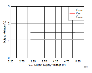
| VOC | TX DC output common mode voltage | RL = 100 Ω, see Figure 26 | 1.125 | 1.2 | 1.375 | V |
| ∆VOC | TX DC common mode voltage difference | RL = 100 Ω, see Figure 26 | –25 | 0 | 25 | mV |
| IOS | TX output short circuit current through OUTx | OUTx = 0 | 10 | mA | ||
| OUTxP = OUTxM | 10 | |||||
| IOZ | TX output current when in high impedance | ENx = 0, OUTx from 0 to VCC | –5 | 5 | µA | |
| COUT | TX output pad capacitance on OUTx at 1 MHz | DW package: ENx = 0, DC offset = VCC / 2, Swing = 200 mV, f = 1 MHz |
10 | pF | ||
| DWW package: ENx = 0, DC offset = VCC / 2, Swing = 200 mV, f = 1 MHz |
10 | |||||
| LVDS RX | ||||||
| VIC | RX input common mode voltage | VCC1, VCC2 ≥ 3 V | 0.5 |VID| | 1.2 | 2.4 – 0.5 |VID| | V |
| VCC1, VCC2 < 3 V | 0.5 |VID| | 1.2 | VCCx – 0.6 – 0.5 |VID| | |||
| VIT1 | Positive going RX input differential threshold | Across VIC | 50 | mV | ||
| VIT2 | Negative going RX input differential threshold | Across VIC | –50 | mV | ||
| IINx | Input current on INx | From 0 to VCCx (each input independently) | 10 | 20 | µA | |
| IINxP – IINxM | Input current balance | From 0 to VCCx | –6 | 6 | µA | |
| CIN | RX input pad capacitance on INx at 1 MHz | DW package: DC offset = 1.2 V, Swing = 200 mV, f = 1 MHz |
6.6 | pF | ||
| DWW package: DC offset = 1.2 V, Swing = 200 mV, f = 1 MHz |
7.5 | |||||
6.10 DC Supply Current Characteristics
(over recommended operating conditions unless otherwise noted)| PARAMETER | TEST CONDITIONS | MIN | TYP | MAX | UNIT | ||
|---|---|---|---|---|---|---|---|
| ISO7821LL | |||||||
| ICC1
ICC2 |
Supply current side 1 and side 2 |
2.25 V < VCC1, VCC2 < 3.6 V | EN1 = EN2 = 0, OUTx floating, VID ≥ 50 mV | 2.2 | 3.3 | mA | |
| EN1 = EN2 = 0, OUTx floating, VID ≤ –50 mV | 3.4 | 5.1 | |||||
| EN1 = EN2 = 1, RL = 100-Ω differential, VID ≥ 50 mV | 6.1 | 9.2 | |||||
| EN1 = EN2 = 1, RL = 100-Ω differential, VID ≤ –50 mV | 7.4 | 11.1 | |||||
| EN1 = EN2 = 1, RL = 100-Ω differential, data communication at 1 Mbps |
6.7 | 10.2 | |||||
| EN1 = EN2 = 1, RL = 100-Ω differential, data communication at 50 Mbps |
7.4 | 11.5 | |||||
| EN1 = EN2 = 1, RL = 100-Ω differential, data communication at 100 Mbps |
8.3 | 12.5 | |||||
| 4.5 V < VCC1, VCC2 < 5.5 V |
EN1 = EN2 = 0, OUTx floating, VID ≥ 50 mV | 2.2 | 3.4 | ||||
| EN1 = EN2 = 0, OUTx floating, VID ≤ –50 mV | 3.5 | 5.2 | |||||
| EN1 = EN2 = 1, RL = 100-Ω differential, VID ≥ 50 mV | 6.4 | 9.8 | |||||
| EN1 = EN2 = 1, RL = 100-Ω differential, VID ≤ –50 mV | 7.8 | 11.7 | |||||
| EN1 = EN2 = 1, RL = 100-Ω differential, data communication at 1 Mbps |
7.1 | 10.8 | |||||
| EN1 = EN2 = 1, RL = 100-Ω differential, data communication at 50 Mbps |
8.1 | 12.1 | |||||
| EN1 = EN2 = 1, RL = 100-Ω differential, data communication at 100 Mbps |
9.5 | 14.1 | |||||
| ISO7820LL | |||||||
| ICC1 | Supply current side 1 |
2.25 V < VCC1, VCC2 < 3.6 V | EN1 = EN2 = 0, OUTx floating, VID ≥ 50 mV | 2.7 | 4.3 | mA | |
| EN1 = EN2 = 0, OUTx floating, VID ≤ –50 mV | 5.3 | 7.9 | |||||
| EN1 = EN2 = 1, RL = 100-Ω differential, VID≥ 50 mV | 2.7 | 4.2 | |||||
| EN1 = EN2 = 1, RL = 100-Ω differential, VID ≤ –50 mV | 5.2 | 8 | |||||
| EN1 = EN2 = 1, RL = 100-Ω differential, data communication at 1 Mbps |
4 | 6.1 | |||||
| EN1 = EN2 = 1, RL = 100-Ω differential, data communication at 50 Mbps |
4.1 | 6.2 | |||||
| EN1 = EN2 = 1, RL = 100-Ω differential, data communication at 100 Mbps |
4.3 | 6.4 | |||||
| 4.5 V < VCC1, VCC2 < 5.5 V |
EN1 = EN2 = 0, OUTx floating, VID ≥ 50 mV | 2.8 | 4.4 | ||||
| EN1 = EN2 = 0, OUTx floating, VID ≤ –50 mV | 5.5 | 8.2 | |||||
| EN1 = EN2 = 1, RL = 100-Ω differential, VID ≥ 50 mV | 2.9 | 4.5 | |||||
| EN1 = EN2 = 1, RL = 100-Ω differential, VID ≤ –50 mV | 5.5 | 8.2 | |||||
| EN1 = EN2 = 1, RL = 100-Ω differential, data communication at 1 Mbps |
4.2 | 6.3 | |||||
| EN1 = EN2 = 1, RL = 100-Ω differential, data communication at 50 Mbps |
4.3 | 6.4 | |||||
| EN1 = EN2 = 1, RL = 100-Ω differential, data communication at 100 Mbps |
4.5 | 6.6 | |||||
| ISO7820LL (continued) | |||||||
| ICC2 | Supply current side 2 |
2.25 V < VCC1, VCC2 < 3.6 V | EN1 = EN2 = 0, OUTx floating, VID ≥ 50 mV | 1.1 | 1.7 | mA | |
| EN1 = EN2 = 0, OUTx floating, VID ≤ –50 mV | 1.1 | 1.7 | |||||
| VID≥ 50 mV | 9.1 | 13.7 | |||||
| EN1 = EN2 = 1, RL = 100-Ω differential, VID ≤ –50 mV | 9.2 | 13.9 | |||||
| EN1 = EN2 = 1, RL = 100-Ω differential, data communication at 1 Mbps |
9.2 | 13.8 | |||||
| EN1 = EN2 = 1, RL = 100-Ω differential, data communication at 50 Mbps |
10.3 | 15.5 | |||||
| EN1 = EN2 = 1, RL = 100-Ω differential, data communication at 100 Mbps |
12.1 | 17.9 | |||||
| 4.5 V < VCC1, VCC2 < 5.5 V |
EN1 = EN2 = 0, OUTx floating, VID ≥ 50 mV | 1.2 | 1.8 | ||||
| EN1 = EN2 = 0, OUTx floating, VID ≤ –50 mV | 1.2 | 1.8 | |||||
| EN1 = EN2 = 1, RL = 100-Ω differential, VID ≥ 50 mV | 9.7 | 14.7 | |||||
| EN1 = EN2 = 1, RL = 100-Ω differential, VID ≤ –50 mV | 9.7 | 14.8 | |||||
| EN1 = EN2 = 1, RL = 100-Ω differential, data communication at 1 Mbps |
9.7 | 14.7 | |||||
| EN1 = EN2 = 1, RL = 100-Ω differential, data communication at 50 Mbps |
11.5 | 17.3 | |||||
| EN1 = EN2 = 1, RL = 100-Ω differential, data communication at 100 Mbps |
14.2 | 21 | |||||
6.11 Switching Characteristics
(over recommended operating conditions unless otherwise noted)| PARAMETER | TEST CONDITIONS | MIN | TYP | MAX | UNIT | |
|---|---|---|---|---|---|---|
| LVDS CHANNEL | ||||||
| tPLH
tPHL |
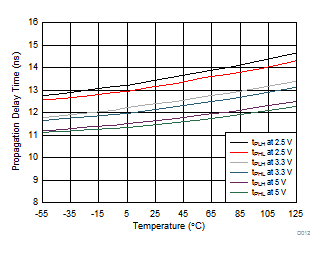
Propagation delay time | 17 | 25 | ns | ||
| PWD | Pulse width distortion |tPHL – tPLH| | 0 | 4.5 | ns | ||
| tsk(o) | Channel-to-channel output skew time | Same directional channels, same voltage and temperature | 2.5 | ns | ||
| tsk(pp) | Part-part skew | Same directional channels, same voltage and temperature | 4.5 | ns | ||
| tCMset | Common-mode settling time after EN = 0 to EN = 1 transition. |
Common-mode capacitive load = 100 pF to 0.5 nF |
20 | µs | ||
| tfs | Default output delay time from input power loss | Measured from the time VCC goes below 1.7 V, see Figure 24 | 0.2 | 9 | µs | |
| tie | Time interval error, or peak-to-peak jitter |
216 – 1 PRBS data at 100 Mbps; RX VID = 350 mVPP, 1 ns trf 10% to 90%, TA = 25°C, VCC1, VCC2 = 3.3 V |
1 | ns | ||
| LVDS TX AND RX | ||||||
| trf | TX differential rise/fall times (20% to 80%) | See Figure 22 | 300 | 780 | 1380 | ps |
| ∆VOC(pp) | TX common-mode voltage peak-to-peak at 100 Mbps | 0 | 150 | mVPP | ||
| tPLZ, tPHZ | TX disable time—valid output to HiZ | See Figure 23 | 10 | 20 | ns | |
| tPZH | Enable propagation delay, high impedance-to-high output | See Figure 23 | 10 | 20 | ns | |
| tPZL | Enable propagation delay, high impedance-to-low output | See Figure 23 | 2 | 2.5 | μs | |
| |VID| | Magnitude of RX input differential voltage for valid operation | Driven with voltage sources on RX pins, see the figures in the Parameter Measurement Information section | 100 | 600 | mV | |
| trf(RX) | Allowed RX input differential rise and fall times (20% to 80%) | See Figure 27 | 1 | 0.3 × UI(1) | ns | |
6.12 Insulation Characteristics Curves
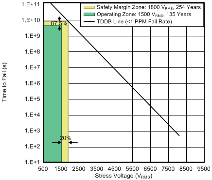
| TA upto 150°C | Operating lifetime = 135 years | |
| Stress-voltage frequency = 60 Hz | ||
| Isolation working voltage = 1500 VRMS | ||
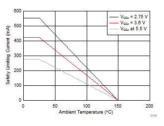 Figure 3. Thermal Derating Curve for Limiting Current for DW Package
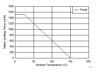 Figure 5. Thermal Derating Curve for Limiting Power for DW Package
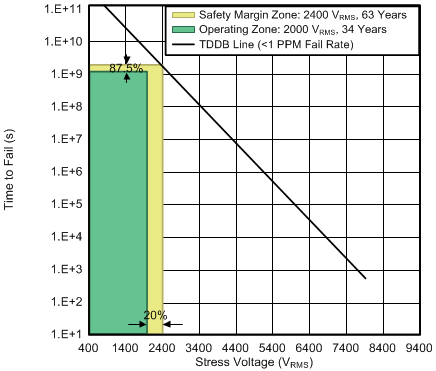
| TA upto 150°C | Operating lifetime = 34 years | |
| Stress-voltage frequency = 60 Hz | ||
| Isolation working voltage = 2000 VRMS | ||
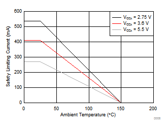 Figure 4. Thermal Derating Curve for Limiting Current for DWW Package
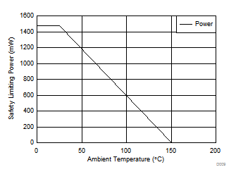 Figure 6. Thermal Derating Curve for Limiting Power for DWW Package
6.13 Typical Characteristics
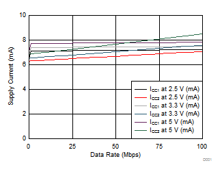
| TA = 25°C | CH-A toggle |
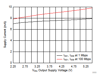
| TA = 25°C |
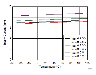
| Data rate = 100 Mbps | CH-B toggle |
(CH-B)
| TA = 25°C | CH-B toggle |
(CH-B)
| Data rate = 100 Mbps | CH-A toggle |
(CH-A)
| TA = 25°C |
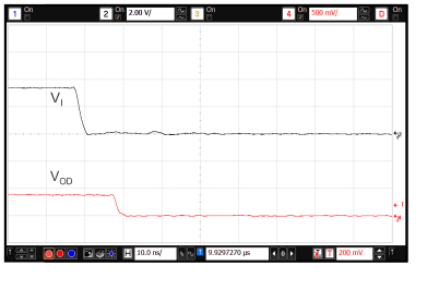 Figure 21. Disable Time (tPLZ, tPHZ)
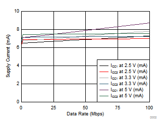
| TA = 25°C | CH-B toggle |
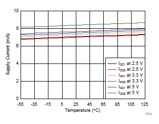
| Data rate = 100 Mbps | CH-A toggle |
(CH-A)
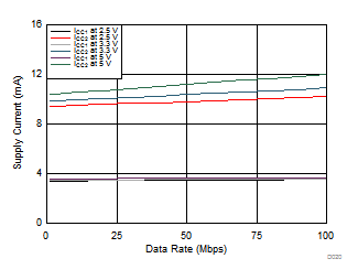
| TA = 25°C | CH-A toggle |
(CH-A)
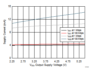
| TA = 25°C |
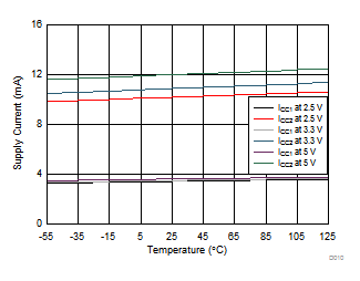
| Data rate = 100 Mbps | CH-B toggle |
(CH-B)
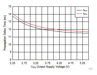
| TA = 25°C |
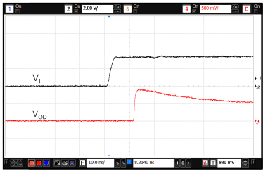
7 Parameter Measurement Information

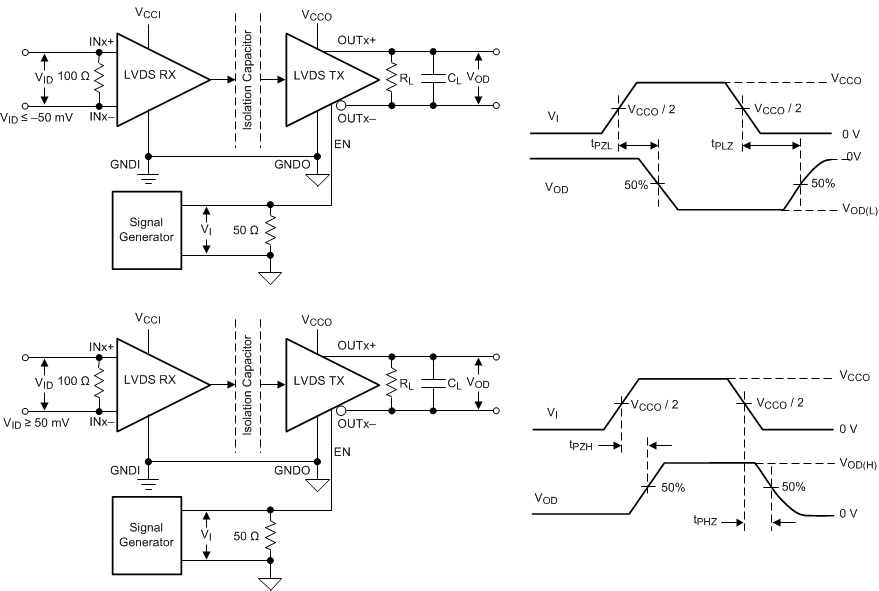
tr ≤ 3 ns, tf ≤ 3 ns, ZO = 50 Ω.

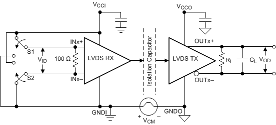
 Figure 26. Driver Test Circuit
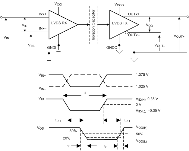 Figure 27. Voltage Definitions and Waveforms
8 Detailed Description
8.1 Overview
The ISO782xLL is a family of isolated LVDS buffers. The differential signal received on the LVDS input pins is first converted to CMOS logic levels. The signal is then transmitted across a silicon-dioxide (SiO2) based capacitive-isolation barrier using an on-off keying (OOK) modulation scheme. A high frequency carrier transmitted across the barrier represents one logic state and an absence of a carrier represents the other logic state. On the other side of the barrier a demodulator converts the OOK signal back to logic levels, which is then converted to LVDS outputs by a differential driver. These devices incorporate advanced circuit techniques to maximize CMTI performance and minimize radiated emissions.
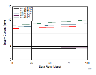
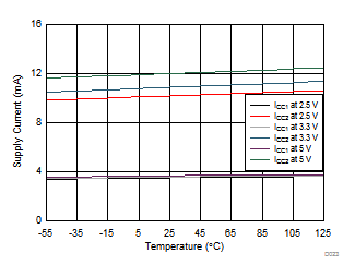
The ISO782xLL family of devices is TIA/EIA-644-A standard compliant. The LVDS transmitters drive a minimum differential-output voltage magnitude of 250 mV into a 100-Ω load, and the LVDS receivers are capable of detecting differential signals ≥50 mV in magnitude. The device consumes 10 mA per channel at 100 Mbps with 5-V supplies.
The Functional Block Diagram section shows a conceptual block diagram of one channel of the ISO782xLL family of devices.
8.2 Functional Block Diagram
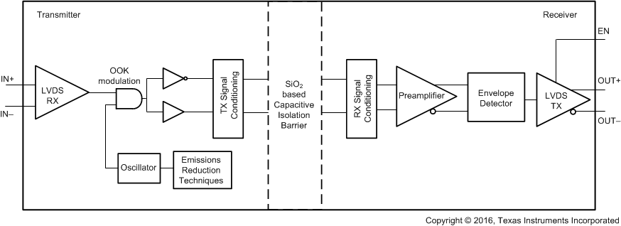
8.3 Feature Description
The ISO782xLL family of devices is available in two channel configurations with a default differential high-output state.
| PART NUMBER | CHANNEL DIRECTION | RATED ISOLATION | MAXIMUM DATA RATE | DEFAULT DIFFERENTIAL OUTPUT |
|---|---|---|---|---|
| ISO7820LL | 2 Forward | 5700 VRMS / 8000 VPK (1) | 100 Mbps | High |
| ISO7821LL | 1 Forward, 1 Reverse |
8.4 Device Functional Modes
Table 1 lists the functional modes for the ISO782xLL family of devices.
Table 1. ISO782xLL Function Table(1)
| VCCI | VCCO | INPUT (INx±)(2) |
OUTPUT ENABLE (ENx) |
OUTPUT (OUTx±)(3) |
COMMENTS |
|---|---|---|---|---|---|
| PU | PU | H | H or open | H | Normal Operation: A channel output assumes the logic state of the input. |
| L | H or open | L | |||
| I | H or open | H or L | |||
| X | PU | X | L | Z | A low-logic state at the output enable causes the outputs to be in high impedance. |
| PD | PU | X | H or open | H | Default mode: When VCCI is unpowered, a channel output assumes the logic high state. When VCCI transitions from unpowered to powered up, a channel output assumes the logic state of the input. When VCCI transitions from powered up to unpowered, a channel output assumes the selected default high state. |
| X | PD | X | X | Undetermined | When VCCO is unpowered, a channel output is undetermined. When VCCO transitions from unpowered to powered-up, a channel output assumes the logic state of the input |
8.4.1 Device I/O Schematics
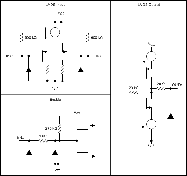 Figure 28. Device I/O Schematics