-
LP5912-Q1 汽车类 500mA 低噪声、低 IQ LDO
- 1 特性
- 2 应用
- 3 说明
- 4 修订历史记录
- 5 Voltage Options
- 6 Pin Configuration and Functions
- 7 Specifications
- 8 Detailed Description
- 9 Applications and Implementation
- 10Power Supply Recommendations
- 11Layout
- 12器件和文档支持
- 13机械、封装和可订购信息
- 重要声明
LP5912-Q1 汽车类 500mA 低噪声、低 IQ LDO
1 特性
- 适用于汽车电子 应用
- 具有符合 AEC Q100 的下列结果:
- 器件温度 1 级:-40℃ 至 +125℃ 的环境运行温度范围
- 器件人体放电模式 (HBM) 分类等级 2
- 器件组件充电模式 (CDM) 分类等级 C6
- 输入电压范围:1.6V 至 6.5V
- 输出电压范围:0.8V 至 5.5V
- 输出电流最高达 500 mA
- 低输出电压噪声:12µVRMS 典型值
- 1kHz 时的电源抑制比 (PSRR):75dB(典型值)
- 输出电压容差 (VOUT ≥ 3.3V):±2%
- 低 IQ(使能时,无负载):30µA(典型值)
- 低压降 (VOUT ≥ 3.3V):500mA 负载时典型值为 95mV
- 与 1µF 陶瓷输入和输出电容搭配使用,性能稳定
- 热过载保护和短路保护
- 反向电流保护
- 无需噪声旁路电容
- 自动输出放电实现快速关断
- 电源正常状态输出具有 140µs 典型延迟
- 内部软启动限制浪涌电流
- –40°C 至 +125°C 的运行结温范围
2 应用
- 车用信息娱乐
- 车载通讯系统
- 高级驾驶员辅助系统 (ADAS) 摄像机和雷达
- 导航系统
3 说明
LP5912-Q1 是一款能提供高达 500mA 输出电流的低噪声 LDO。LP5912-Q1 器件专为满足射频 (RF) 和模拟电路的要求而设计,具备低噪声、高 PSRR、低静态电流以及低线路或负载瞬态响应等特性。LP5912-Q1 无需噪声旁路电容便可提供出色的噪声性能,并且支持远距离安置输出电容。
此器件适合与 1µF 输入和 1µF 输出陶瓷电容搭配使用(无需独立的噪声旁路电容)。
其固定输出电压介于 0.8V 和 5.5V 之间(以 25mV 为单位增量)。如需特定的电压选项,请联系德州仪器 (TI) 销售代表。
器件信息(1)
| 器件型号 | 封装 | 封装尺寸(标称值) |
|---|---|---|
| LP5912-Q1 | WSON (6) | 2.00mm x 2.00mm |
- 要了解所有可用封装,请参见数据表末尾的封装选项附录 (POA)。
空白
空白
空白
空白
空白
简化电路原理图
5 Voltage Options
This device is capable of providing fixed output voltages from 0.8 V to 5.5 V in 25-mV steps. For all available package and voltage options, see the POA at the end of this datasheet. Contact Texas Instruments Sales for specific voltage option needs.
6 Pin Configuration and Functions
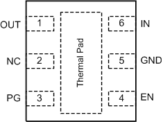
Pin Functions
| PIN | I/O | DESCRIPTION | |
|---|---|---|---|
| NUMBER | NAME | ||
| 1 | OUT | O | Regulated output voltage |
| 2 | NC | — | No internal connection. Leave open, or connect to ground. |
| 3 | PG | O | Power-good indicator. Requires external pullup. |
| 4 | EN | I | Enable input. Logic high = device is ON, logic low = device is OFF, with internal 3-MΩ pulldown. |
| 5 | GND | G | Ground |
| 6 | IN | I | Unregulated input voltage |
| — | Exposed thermal pad | — | Connect to copper area under the package to improve thermal performance. The use of thermal vias to transfer heat to inner layers of the PCB is recommended. Connect the thermal pad to ground, or leave floating. Do not connect the thermal pad to any potential other than ground. |
7 Specifications
7.1 Absolute Maximum Ratings
over operating free-air temperature range (unless otherwise noted)(1)(2)| MIN | MAX | UNIT | ||
|---|---|---|---|---|
| VIN | Input voltage | –0.3 | 7 | V |
| VOUT | Output voltage | –0.3 | 7 | V |
| VEN | Enable input voltage | –0.3 | 7 | V |
| VPG | Power Good (PG) pin OFF voltage | –0.3 | 7 | V |
| TJ | Junction temperature | 150 | °C | |
| PD | Continuous power dissipation(3) | Internally Limited | W | |
| Tstg | Storage temperature | –65 | 150 | °C |
7.2 ESD Ratings
| VALUE | UNIT | |||
|---|---|---|---|---|
| V(ESD) | Electrostatic discharge | Human-body model (HBM), per AEC Q100-002(1) | ±2000 | V |
| Charged-device model (CDM), per AEC Q100-011 | ±1000 | |||
7.3 Recommended Operating Conditions
over operating free-air temperature range (unless otherwise noted)(1)| MIN | MAX | UNIT | ||
|---|---|---|---|---|
| VIN | Input supply voltage | 1.6 | 6.5 | V |
| VOUT | Output voltage | 0.8 | 5.5 | V |
| VEN | Enable input voltage | 0 | VIN | V |
| VPG | PG pin OFF voltage | 0 | 6.5 | V |
| IOUT | Output current | 0 | 500 | mA |
| TJ-MAX-OP | Operating junction temperature(2) | –40 | 125 | °C |
7.4 Thermal Information
| THERMAL METRIC(1) | LP5912-Q1 | UNIT | |
|---|---|---|---|
| DRV (WSON) | |||
| 6 PINS | |||
| RθJA | Junction-to-ambient thermal resistance, High-K(2) | 71.2(3) | °C/W |
| RθJC(top) | Junction-to-case (top) thermal resistance | 93.7 | °C/W |
| RθJB | Junction-to-board thermal resistance | 40.7 | °C/W |
| ψJT | Junction-to-top characterization parameter | 2.5 | °C/W |
| ψJB | Junction-to-board characterization parameter | 41.1 | °C/W |
| ψJC(bot) | Junction-to-case (bottom) thermal resistance | 11.2 | °C/W |
7.5 Electrical Characteristics
VIN = VOUT(NOM) + 0.5 V or 1.6 V, whichever is greater; VEN = 1.3 V, CIN = 1 µF, COUT = 1 µF, IOUT = 1 mA (unless otherwise stated).(1)(2)(3)| PARAMETER | TEST CONDITIONS | MIN | TYP | MAX | UNIT | |
|---|---|---|---|---|---|---|
| OUTPUT VOLTAGE | ||||||
| ΔVOUT | Output voltage tolerance | For VOUT(NOM) ≥ 3.3 V: VOUT(NOM) + 0.5 V ≤ VIN ≤ 6.5 V, IOUT = 1 mA to 500 mA |
–2% | 2% | ||
| For 1.1 V ≤ VOUT(NOM) < 3.3 V: VOUT(NOM) + 0.5 V ≤ VIN ≤ 6.5 V, IOUT = 1 mA to 500 mA |
–3% | 3% | ||||
| For VOUT(NOM) < 1.1 V: 1.6 V ≤ VIN ≤ 6.5 V, IOUT = 1 mA to 500 mA |
||||||
| Line regulation | For VOUT(NOM) ≥ 1.1 V: VOUT(NOM) + 0.5 V ≤ VIN ≤ 6.5 V |
0.8 | %/V | |||
| For VOUT(NOM) < 1.1 V: 1.6 V ≤ VIN ≤ 6.5 V |
||||||
| Load regulation | IOUT = 1 mA to 500 mA | 0.0022 | %/mA | |||
| CURRENT LEVELS | ||||||
| ISC | Short-circuit current limit | TJ = 25°C, see(4) | 700 | 900 | 1100 | mA |
| IRO | Reverse leakage current(5) | VIN < VOUT | 10 | 150 | µA | |
| IQ | Quiescent current(6) | VEN = 1.3 V, IOUT = 0 mA | 30 | 55 | µA | |
| VEN = 1.3 V, IOUT = 500 mA | 400 | 600 | ||||
| IQ(SD) | Quiescent current, shutdown mode(6) | VEN = 0 V –40°C ≤ TJ ≤ 85°C |
0.2 | 1.5 | µA | |
| VEN = 0 V | 0.2 | 5 | ||||
| IG | Ground current(7) | VEN = 1.3 V, IOUT = 0 mA | 35 | µA | ||
| VDO DROPOUT VOLTAGE | ||||||
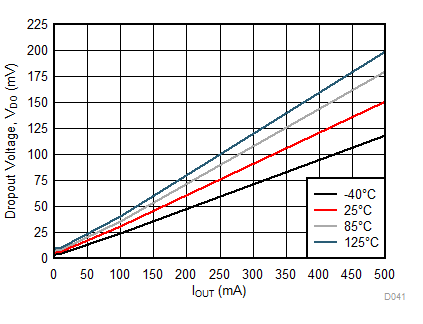
| VDO | Dropout voltage(8) | IOUT = 500 mA, 1.6 V ≤ VOUT(NOM) < 3.3 V | 170 | 250 | mV | |
| IOUT = 500 mA, 3.3 V ≤ VOUT(NOM) ≤ 5.5 V | 95 | 180 | mV | |||
| VIN to VOUT RIPPLE REJECTION | ||||||
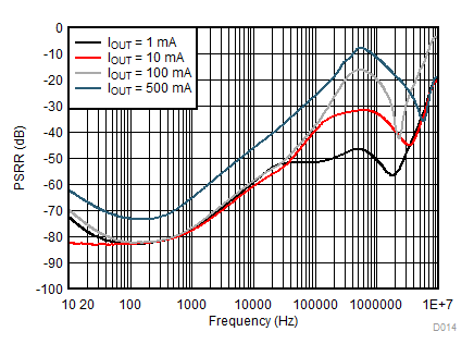
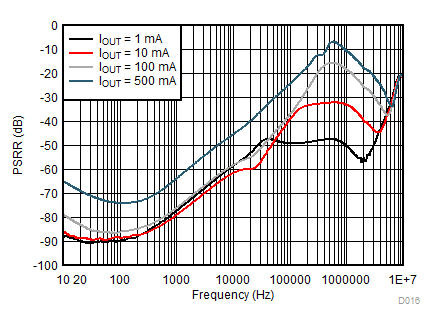
| PSRR | Power Supply Rejection Ratio(10) | ƒ = 100 Hz, VOUT ≥ 1.1 V, IOUT = 20 mA | 80 | dB | ||
| ƒ = 1 kHz, VOUT ≥ 1.1 V, IOUT = 20 mA | 75 | |||||
| ƒ = 10 kHz, VOUT ≥ 1.1 V, IOUT = 20 mA | 65 | |||||
| ƒ = 100 kHz, VOUT ≥ 1.1 V, IOUT = 20 mA | 40 | |||||
| ƒ = 100 Hz, 0.8 V < VOUT < 1.1 V, IOUT = 20 mA | 65 | |||||
| ƒ = 1 kHz, 0.8 V < VOUT < 1.1 V, IOUT = 20 mA | 65 | |||||
| ƒ = 10 kHz, 0.8 V < VOUT < 1.1 V, IOUT = 20 mA | 65 | |||||
| ƒ = 100 kHz, 0.8 V < VOUT < 1.1 V, IOUT = 20 mA | 40 | |||||
| OUTPUT NOISE VOLTAGE | ||||||
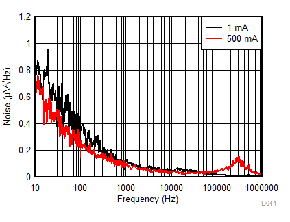
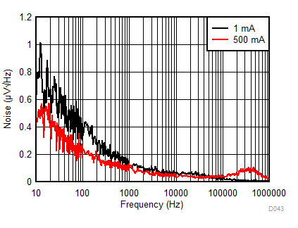
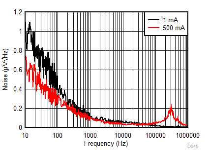
| eN | Noise voltage | IOUT = 1 mA, BW = 10 Hz to 100 kHz | 12 | µVRMS | ||
| IOUT = 500 mA, BW = 10 Hz to 100 kHz | 12 | |||||
| THERMAL SHUTDOWN | ||||||
| TSD | Thermal shutdown temperature | 160 | °C | |||
| THYS | Thermal shutdown hysteresis | 15 | °C | |||
| LOGIC INPUT THRESHOLDS | ||||||
| VEN(OFF) | OFF threshold | VIN = 1.6 V to 6.5 V VEN falling until device is disabled |
0.3 | V | ||
| VEN(ON) | ON threshold | 1.6 V ≤ VIN ≤ 6.5 V VEN rising until device is enabled |
1.3 | |||
| IEN | Input current at EN pin(9) | VEN = 6.5 V, VIN = 6.5 V | 2.5 | µA | ||
| VEN = 0 V, VIN = 3.3 V | 0.001 | |||||
| PGHTH | PG high threshold (% of nominal VOUT) | 94% | ||||
| PGLTH | PG low threshold (% of nominal VOUT) | 90% | ||||
| VOL(PG) | PG pin low-level output voltage | VOUT < PGLTH, sink current = 1 mA | 100 | mV | ||
| IlKG(PG) | PG pin leakage current | VOUT < PGHTH, VPG = 6.5 V | 1 | µA | ||
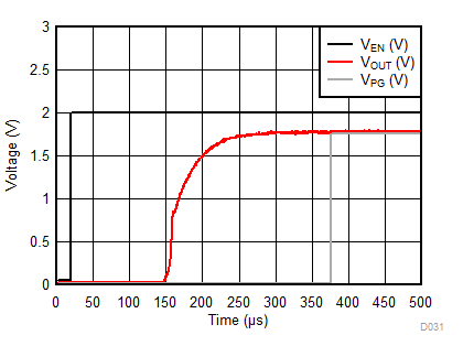
| tPGD | PG delay time | Time from VOUT > PG threshold to PG toggling | 140 | µs | ||
| TRANSITION CHARACTERISTICS | ||||||
| ΔVOUT | Line transients(10) | For VIN ↑ and VOUT(NOM) ≥ 1.1 V: VIN = (VOUT(NOM) + 0.5 V) to (VOUT(NOM) + 1.1 V), VIN trise = 30 µs |
1 | mV | ||
| For VIN ↑ and VOUT(NOM) < 1.1 V: VIN = 1.6 V to 2.2 V, VIN trise = 30 µs |
||||||
| For VIN ↓ and VOUT(NOM) ≥ 1.1 V: VIN = (VOUT(NOM) + 1.1 V) to (VOUT(NOM) + 0.5 V) VIN tfall = 30 µs |
–1 | |||||
| For VIN ↓ and VOUT(NOM) < 1.1 V: VIN = 2.2 V to 1.6 V VIN tfall = 30 µs |
||||||
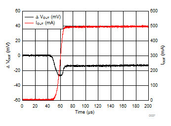
| Load transients(10) | IOUT = 5 mA to 500 mA IOUT trise = 10 µs |
–45 | mV | |||
| IOUT = 500 mA to 5 mA IOUT tfall = 10 µs |
45 | |||||
| Overshoot on start-up(10) | Stated as a percentage of VOUT(NOM) | 5% | ||||
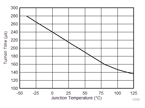
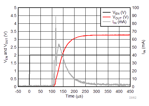
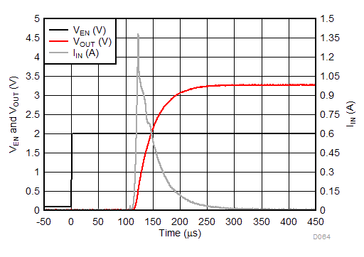
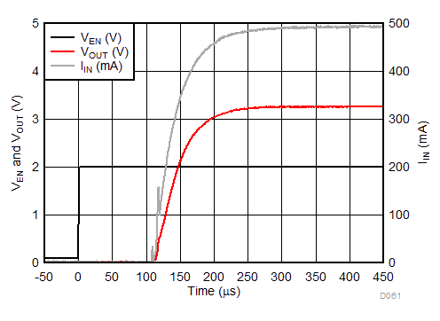
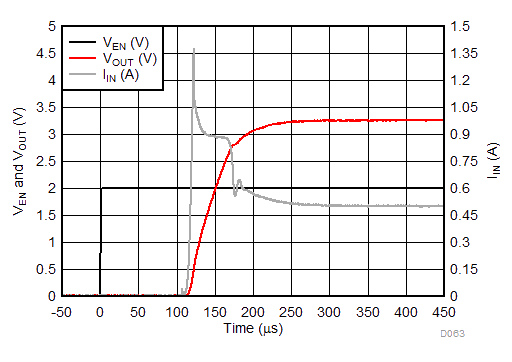
| tON | Turnon time | From VEN > VEN(ON) to VOUT = 95% of VOUT(NOM) | 200 | µs | ||
| OUTPUT AUTO DISCHARGE RATE | ||||||
| RAD | Output discharge pulldown resistance | VEN = 0 V, VIN = 3.6 V | 100 | Ω | ||
7.6 Output and Input Capacitors
over operating free-air temperature range (unless otherwise noted)| PARAMETER | TEST CONDITIONS | MIN(1) | TYP | MAX | UNIT | |
|---|---|---|---|---|---|---|
| CIN | Input capacitance(2) | Capacitance for stability | 0.7 | 1 | µF | |
| COUT | Output capacitance(2) | 0.7 | 1 | 10 | µF | |
| ESR | Output voltage(2) | 5 | 500 | mΩ | ||
7.7 Typical Characteristics
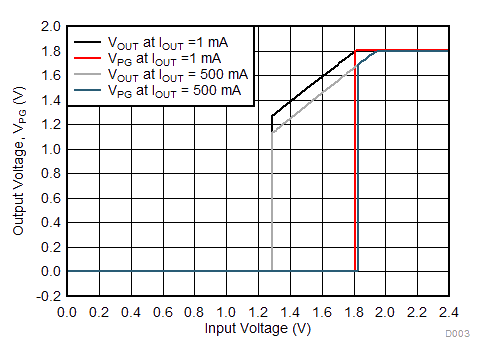
Unless otherwise stated: VIN = VOUT + 0.5 V, VEN = VIN, IOUT = 1 mA, CIN = 1 µF, COUT = 1 µF, TJ = 25°C, unless otherwise stated.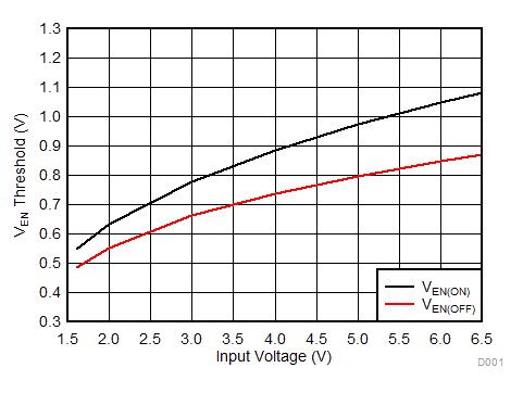
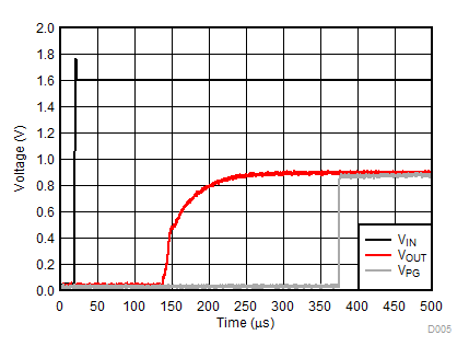
| VIN = 0 V to 1.6 V | IOUT = 1 mA | |

| VIN = 0 V to 2.3 V | IOUT = 1 mA | |
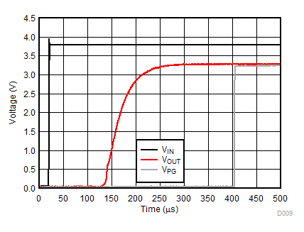
| VIN = 0 V to 3.8 V | IOUT = 1 mA | |
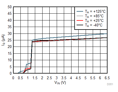
| IOUT = 0 mA |
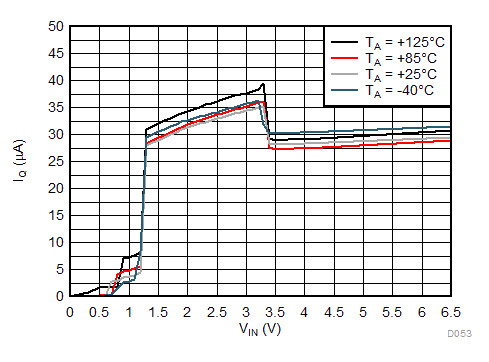
| IOUT = 0 mA | ||
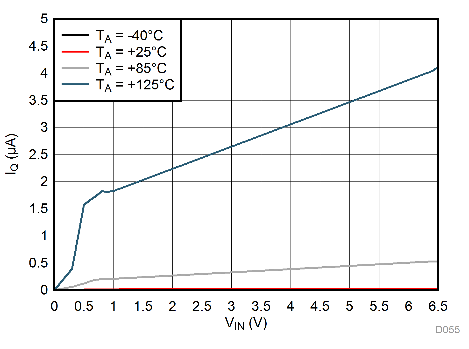
| VEN = 0 V |
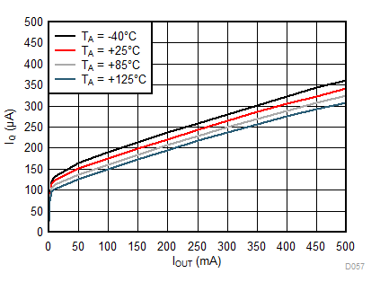
| VIN = 1.6 V |
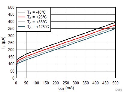
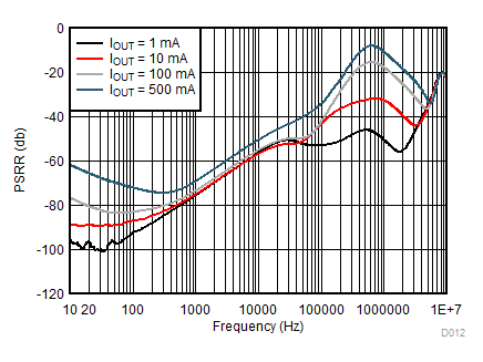
| VIN = 1.6 V | ||
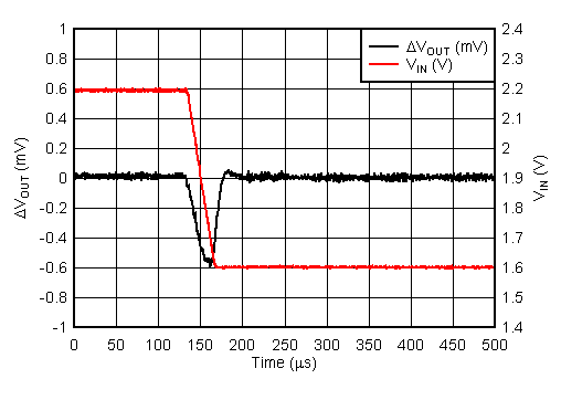
| VIN = 2.2 V to 1.6 V | tfall = 30 µs | |
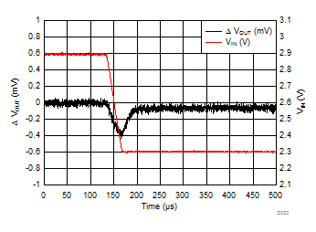
| VIN = 2.9 V to 2.3 V | tfall = 30 µs | |
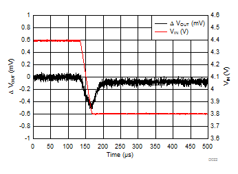
| VIN = 4.4 V to 3.8 V | tfall = 30 µs | |
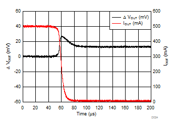
| VIN = 1.6 V | IOUT = 500 mA to 5 mA | tfall = 10 µs |
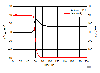
| IOUT = 500 mA to 5 mA | tfall = 10 µs | |
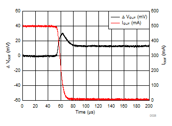
| IOUT = 500 mA to 5 mA | tfall = 10 µs | |
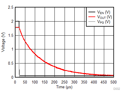
| IOUT = 0 mA | COUT = 1 µF |
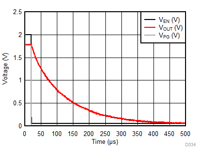
| IOUT = 1 mA | COUT = 1 µF |
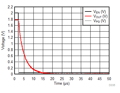
| IOUT = 500 mA | COUT = 1 µF |
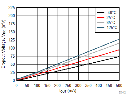
| IOUT = 0 mA (No Load) |
| CIN = Open | IOUT = 1 mA | COUT = 1 µF |
| CIN = Open | IOUT = 1 mA | COUT = 10 µF | ||
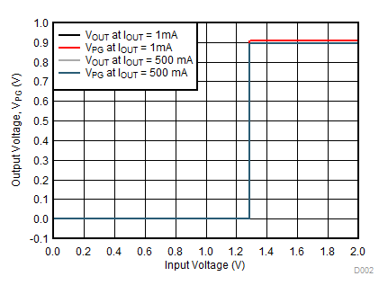
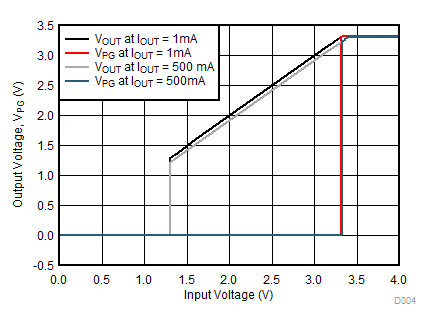
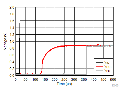
| VIN = 0 V to 1.6 V | IOUT = 500 mA | |
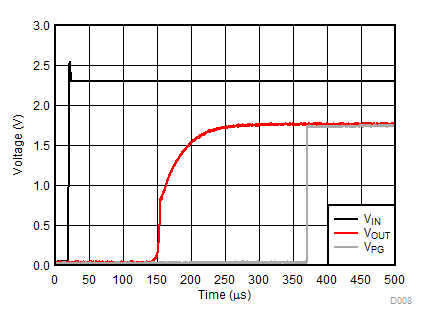
| VIN = 0 V to 2.3 V | IOUT = 500 mA | |
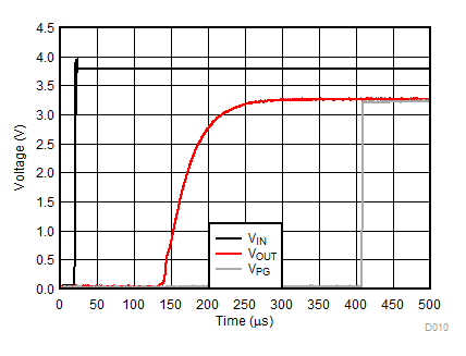
| VIN = 0 V to 3.8 V | IOUT = 500 mA | |
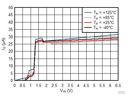
| IOUT = 0 mA |
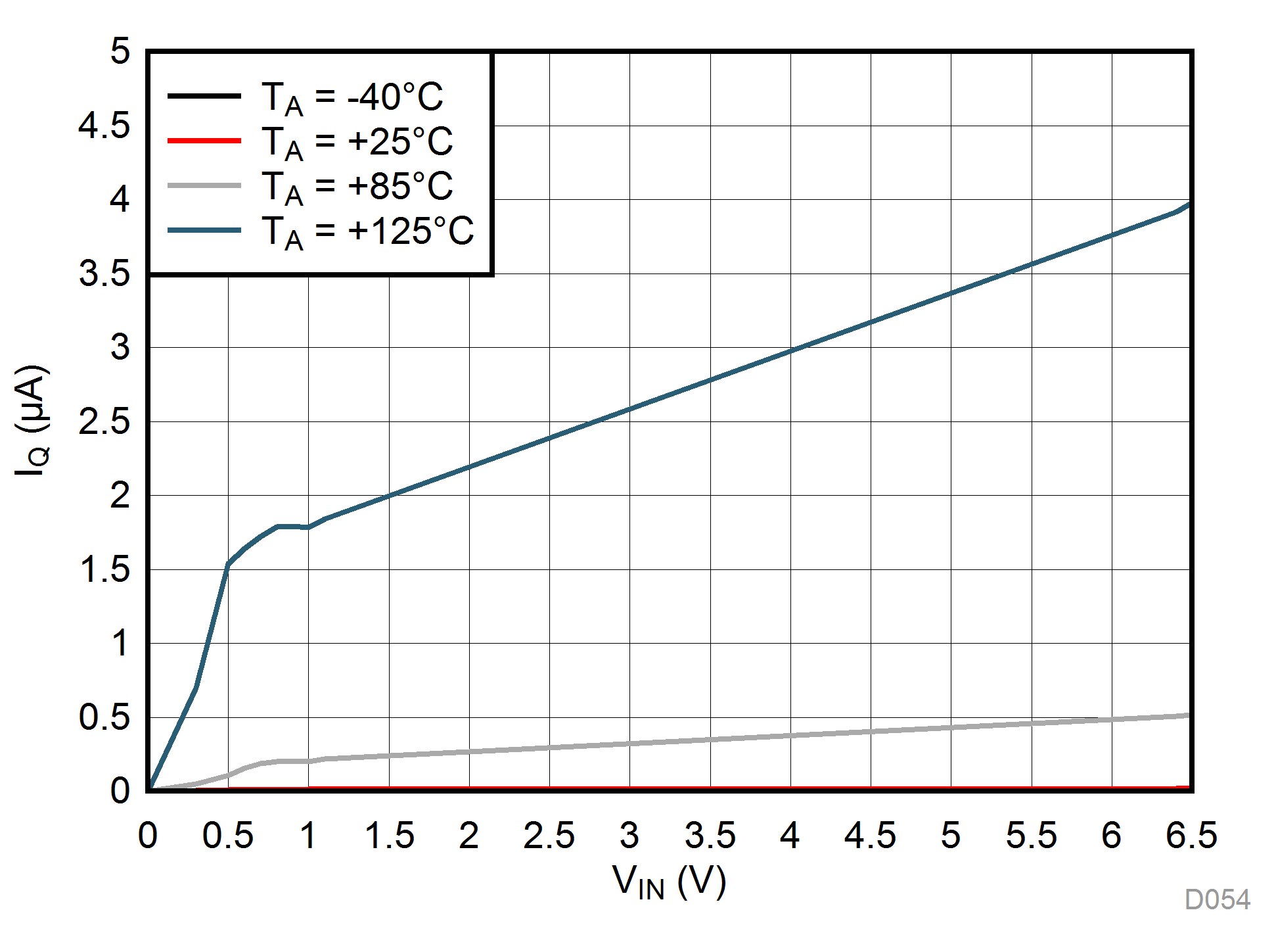
| VEN = 0 V |

| VEN = 0 V |
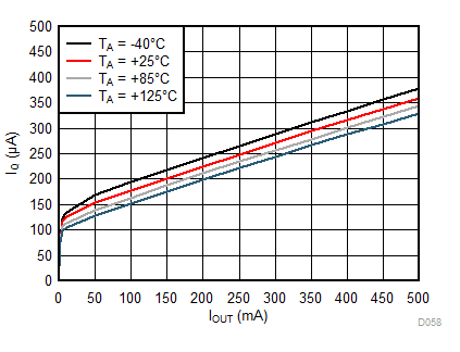
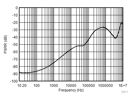
| VIN = 1.6 V | IOUT = 20 mA | |
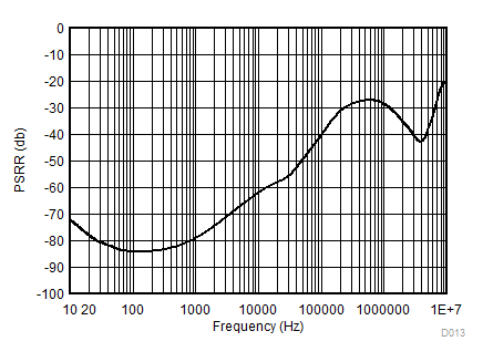
| IOUT = 20 mA | ||
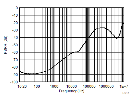
| IOUT = 20 mA | ||
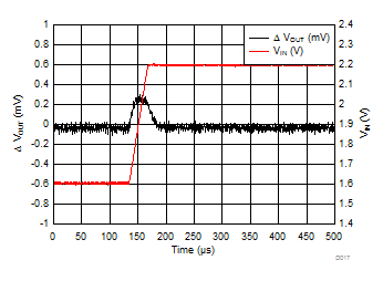
| VIN = 1.6 V to 2.2 V | trise = 30 µs | |
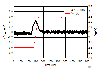
| VIN = 2.3 V to 2.9 V | trise = 30 µs | |
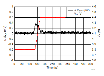
| VIN = 3.8 V to 4.4 V | trise = 30 µs | |
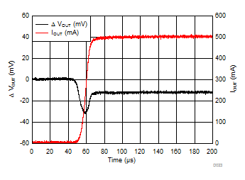
| VIN = 1.6 V | IOUT = 5 mA to 500 mA | trise = 10 µs |
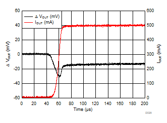
| IOUT = 5 mA to 500 mA | trise = 10 µs | |
| IOUT = 5 mA to 500 mA | trise = 10 µs | |
| IOUT = 0 mA | COUT = 1 µF | |

| IOUT = 1 mA | COUT = 1 µF |

| IOUT = 500 mA | COUT = 1 µF |
| VIN = 1.6 V |
| CIN = Open | IOUT = 500 mA | COUT = 1 µF |
| CIN = Open | IOUT = 500 mA | COUT = 10 µF |
8 Detailed Description
8.1 Overview
The LP5912-Q1 is a low-noise, high PSRR, LDO capable of sourcing a 500-mA load. The LP5912-Q1 can operate down to 1.6-V input voltage and 0.8-V output voltage. This combination of low noise, high PSRR, and low output voltage makes the device an ideal low dropout (LDO) regulator to power a multitude of loads from noise-sensitive communication components to battery-powered system.
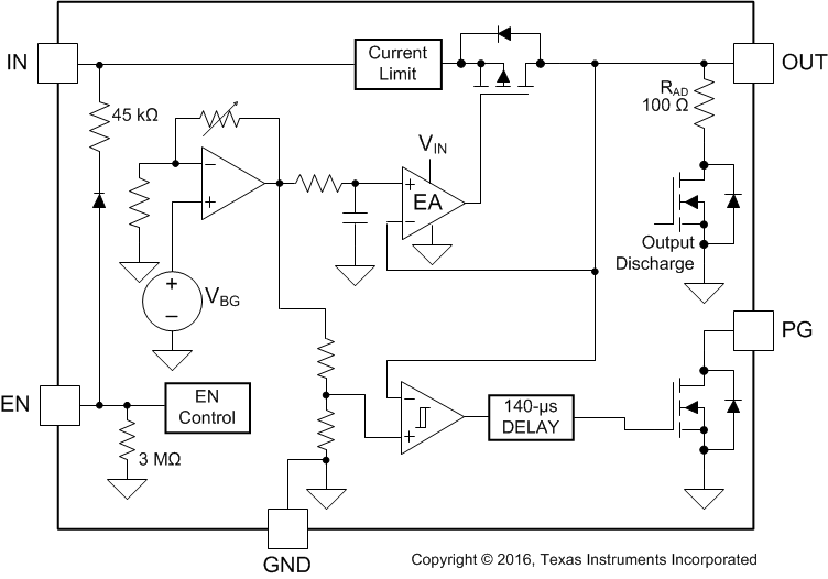
The LP5912-Q1 Functional Block Diagram contains several features, including:
8.2 Functional Block Diagram
8.3 Feature Description
8.3.1 Enable (EN)
The LP5912-Q1 EN pin is internally held low by a 3-MΩ resistor to GND. The EN pin voltage must be higher than the VEN(ON) threshold to ensure that the device is fully enabled under all operating conditions. The EN pin voltage must be lower than the VEN(OFF) threshold to ensure that the device is fully disabled and the automatic output discharge is activated.
When the device is disabled the output stage is disabled, the PG output pin is low, and the output automatic discharge is ON.
8.3.2 Output Automatic Discharge (RAD)
The LP5912-Q1 output employs an internal 100-Ω (typical) pulldown resistance to discharge the output when the EN pin is low. Note that if the LP5912-Q1 EN pin is low (the device is OFF) and the OUT pin is held high by a secondary supply, current flows from the secondary supply through the automatic discharge pulldown resistor to ground.
8.3.3 Reverse Current Protection (IRO)
The LP5912-Q1 input is protected against reverse current when output voltage is higher than the input. In the event that extra output capacitance is used at the output, a power-down transient at the input would normally cause a large reverse current through a conventional regulator. The LP5912-Q1 includes a reverse voltage detector that trips when VIN drops below VOUT, shutting off the regulator and opening the PMOS body diode connection, preventing any reverse current from the OUT pin from flowing to the IN pin.
If the LP5912 EN pin is low (the LP5912 is OFF) and the OUT pin is held high by a secondary supply, current flows from the secondary supply through the automatic discharge pulldown resistor to ground. This is not reverse current, this is automatic discharge pulldown current.
Note that reverse current (IRO) is measured at the IN pin.
8.3.4 Internal Current Limit (ISC)
The internal current limit circuit is used to protect the LDO against high-load current faults or shorting events. The LDO is not designed to operate continuously at the ISC current limit. During a current-limit event, the LDO sources constant current. Therefore, the output voltage falls when load impedance decreases. Note also that if a current limit occurs and the resulting output voltage is low, excessive power may be dissipated across the LDO, resulting in a thermal shutdown of the output.
8.3.5 Thermal Overload Protection (TSD)
Thermal shutdown disables the output when the junction temperature rises to approximately 160°C, which allows the device to cool. When the junction temperature cools to approximately 145°C, the output circuitry enables. Based on power dissipation, thermal resistance, and ambient temperature, the thermal protection circuit may cycle on and off. This thermal cycling limits the dissipation of the regulator and protects it from damage as a result of overheating.
8.3.6 Power-Good Output (PG)
The LP5912-Q1 device has a power-good function that works by toggling the state of the PG output pin. When the output voltage falls below the PG threshold voltage (PGLTH), the PG pin open-drain output engages (low impedance to GND). When the output voltage rises above the PG threshold voltage (PGVHTH), the PG pin becomes high impedance. By connecting a pullup resistor to an external supply, any downstream device can receive PG as a logic signal. Make sure that the external pullup supply voltage results in a valid logic signal for the receiving device or devices. Use a pullup resistor from 10 kΩ to 100 kΩ for best results.
The input supply, VIN, must be no less than the minimum operating voltage of 1.6 V to ensure that the PG pin output status is valid. The PG pin output status is undefined when VIN is less than 1.6 V.
In power-good function, the PG output pin being pulled high is typically delayed 140 µs after the output voltage rises above the PGHTH threshold voltage. If the output voltage rises above the PGHTH threshold and then falls below the PGLTH threshold voltage the PG pin falls immediately with no delay time.
If the PG function is not needed, the pullup resistor can be eliminated, and the PG pin can be either connected to ground or left floating.
8.4 Device Functional Modes
8.4.1 Enable (EN)
The LP5912-Q1 EN pin is internally held low by a 3-MΩ resistor to GND. The EN pin voltage must be higher than the VEN(ON) threshold to ensure that the device is fully enabled under all operating conditions. When the EN pin voltage is lower than the VEN(OFF) threshold, the output stage is disabled, the PG pin goes low, and the output automatic discharge circuit is activated. Any charge on the OUT pin is discharged to ground through the internal 100-Ω (typical) output auto discharge pulldown resistance.
8.4.2 Minimum Operating Input Voltage (VIN)
The LP5912-Q1 device does not include any dedicated UVLO circuit. The device internal circuit is not fully functional until VIN is at least 1.6 V. The output voltage is not regulated until VIN has reached at least the greater of 1.6 V or (VOUT + VDO).
9 Applications and Implementation
NOTE
Information in the following applications sections is not part of the TI component specification, and TI does not warrant its accuracy or completeness. TI’s customers are responsible for determining suitability of components for their purposes. Customers must validate and test their design implementation to confirm system functionality.
9.1 Application Information
The LP5912-Q1 is designed to meet the requirements of RF and analog circuits, by providing low noise, high PSRR, low quiescent current, and low line or load transient response. The device offers excellent noise performance without the need for a noise bypass capacitor and is stable with input and output capacitors with a value of 1 μF. The device delivers this performance in an industry standard WSON package, which for this device is specified with an operating junction temperature (TJ) of –40°C to +125°C.
9.2 Typical Application
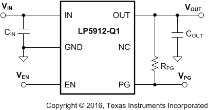
Figure 54 shows the typical application circuit for the LP5912-Q1. Input and output capacitances may need to be increased above the 1-μF minimum for some applications.
 Figure 54. LP5912-Q1 Typical Application
9.2.1 Design Requirements
For typical RF linear regulator applications, use the parameters listed in Table 1.
Table 1. Design Parameters
| DESIGN PARAMETER | EXAMPLE VALUE |
|---|---|
| Input voltage | 1.6 to 6.5 V |
| Output voltage | 0.8 to 5.5 V |
| Output current | 500 mA |
| Output capacitor | 1 to 10 µF |
| Input/output capacitor ESR range | 5 mΩ to 500 mΩ |
9.2.2 Detailed Design Procedure
9.2.2.1 External Capacitors
Like most low-dropout regulators, the LP5912-Q1 requires external capacitors for regulator stability. The device is specifically designed for portable applications requiring minimum board space and smallest components. These capacitors must be correctly selected for good performance.
9.2.2.2 Input Capacitor
An input capacitor is required for stability. The input capacitor must be at least equal to, or greater than, the output capacitor for good load-transient performance. A capacitor of at least 1 µF must be connected between the LP5912-Q1 IN pin and ground for stable operation over full load-current range. It is acceptable to have more output capacitance than input, as long as the input is at least 1 µF.
The input capacitor must be located a distance of not more than 1 cm from the input pin and returned to a clean analog ground. Any good-quality ceramic, tantalum, or film capacitor may be used at the input.
NOTE
To ensure stable operation it is essential that good PCB practices are employed to minimize ground impedance and keep input inductance low. If these conditions cannot be met, or if long leads are to be used to connect the battery or other power source to the LP5912-Q1, increasing the value of the input capacitor to at least 10 µF is recommended. Also, tantalum capacitors can suffer catastrophic failures due to surge current when connected to a low-impedance source of power (such as a battery or a very large capacitor). If a tantalum capacitor is used at the input, it must be verified by the manufacturer to have a surge current rating sufficient for the application. There are no requirements for the equivalent series resistance (ESR) on the input capacitor, but tolerance and temperature coefficient must be considered when selecting the capacitor to ensure the capacitance remains 1 μF ±30% over the entire operating temperature range.
9.2.2.3 Output Capacitor
The LP5912-Q1 is designed specifically to work with a very small ceramic output capacitor, typically 1 µF. A ceramic capacitor (dielectric types X5R or X7R) in the 1-µF to 10-µF range, and with an ESR from 5 mΩ to 500 mΩ, is suitable in the LP5912-Q1 application circuit. For this device the output capacitor must be connected between the OUT pin with a good connection back to the GND pin.
Tantalum or film capacitors may also be used at the device output, VOUT, but these are not as attractive for reasons of size and cost (see Capacitor Characteristics).
The output capacitor must meet the requirement for the minimum value of capacitance and have an ESR value that is within the range 5 mΩ to 500 mΩ for stability.
9.2.2.4 Capacitor Characteristics
The LP5912-Q1 is designed to work with ceramic capacitors on the input and output to take advantage of the benefits they offer. For capacitance values in the range of 1 µF to 10 µF, ceramic capacitors are the smallest, least expensive, and have the lowest ESR values, thus making them best for eliminating high frequency noise. The ESR of a typical 1-µF ceramic capacitor is in the range of 20 mΩ to 40 mΩ, which easily meets the ESR requirement for stability for the LP5912-Q1.
The preferred choice for temperature coefficient in a ceramic capacitor is X7R. This type of capacitor is the most stable and holds the capacitance within ±15% over the temperature range. Tantalum capacitors are less desirable than ceramic for use as output capacitors because they are more expensive when comparing equivalent capacitance and voltage ratings in the 1-µF to 10-µF range.
Another important consideration is that tantalum capacitors have higher ESR values than equivalent size ceramics. While it may be possible to find a tantalum capacitor with an ESR value within the stable range, it would have to be larger in capacitance (which means bigger and more costly) than a ceramic capacitor with the same ESR value. Also, the ESR of a typical tantalum increases about 2:1 as the temperature goes from 25°C down to –40°C, so some guard band must be allowed.
9.2.2.5 Remote Capacitor Operation
To ensure stability the LP5912-Q1 requires at least a 1-μF capacitor at the OUT pin. There is no strict requirement about the location of the output capacitor in regards to the LDO OUT pin; the output capacitor may be located 5 to 10 cm away from the LDO. This means that there is no need to have a special capacitor close to the OUT pin if there are already respective capacitors in the system. This placement flexibility requires that the output capacitor be connected directly between the LP5912-Q1 OUT pin and GND pin with no vias. This remote capacitor feature can help users to minimize the number of capacitors in the system.
As a good design practice, keep the wiring parasitic inductance at a minimum, which means using as wide as possible traces from the LDO output to the capacitors, keeping the LDO output trace layer as close to ground layer as possible, avoiding vias on the path. If there is a need to use vias, implement as many as possible vias between the connection layers. Keeping parasitic wiring inductance less than 35 nH is recommended. For applications with fast load transients use an input capacitor equal to, or larger than, the sum of the capacitance at the output node for the best load-transient performance.
9.2.2.6 Power Dissipation
Knowing the device power dissipation and proper sizing of the thermal plane connected to the tab or pad is critical to ensuring reliable operation. Device power dissipation depends on input voltage, output voltage, and load conditions and can be calculated with Equation 1.
Power dissipation can be minimized, and greater efficiency can be achieved, by using the lowest available voltage drop option that is greater than the dropout voltage (VDO). However, keep in mind that higher voltage drops result in better dynamic (that is, PSRR and transient) performance.
On the WSON (DRV) package, the primary conduction path for heat is through the exposed power pad into the PCB. To ensure the device does not overheat, connect the exposed pad, through thermal vias, to an internal ground plane with an appropriate amount of copper PCB area.
Power dissipation and junction temperature are most often related by the junction-to-ambient thermal resistance (RθJA) of the combined PCB and device package and the temperature of the ambient air (TA), according to Equation 2 or Equation 3:
Unfortunately, this RθJA is highly dependent on the heat-spreading capability of the particular PCB design, and therefore varies according to the total copper area, copper weight, and location of the planes. The RθJA recorded in Thermal Information is determined by the specific EIA/JEDEC JESD51-7 standard for PCB and copper-spreading area, and is to be used only as a relative measure of package thermal performance. For a well-designed thermal layout, RθJA is actually the sum of the package junction-to-case (bottom) thermal resistance (RθJCbot) plus the thermal resistance contribution by the PCB copper area acting as a heat sink.
9.2.2.7 Estimating Junction Temperature
The EIA/JEDEC standard recommends the use of psi (Ψ) thermal characteristics to estimate the junction temperatures of surface mount devices on a typical PCB board application. These characteristics are not true thermal resistance values, but rather package specific thermal characteristics that offer practical and relative means of estimating junction temperatures. These psi metrics are determined to be significantly independent of copper-spreading area. The key thermal characteristics (ΨJT and ΨJB) are given in Thermal Information and are used in accordance with Equation 4 or Equation 5.
where
- PD(MAX) is explained in Equation 3
- TTOP is the temperature measured at the center-top of the device package.
where
- PD(MAX) is explained in Equation 3.
- TBOARD is the PCB surface temperature measured 1 mm from the device package and centered on the package edge.
For more information about the thermal characteristics ΨJT and ΨJB, see Semiconductor and IC Package Thermal Metrics ; for more information about measuring TTOP and TBOARD, see Using New Thermal Metrics ; and for more information about the EIA/JEDEC JESD51 PCB used for validating RθJA, see the TI Application Report Thermal Characteristics of Linear and Logic Packages Using JEDEC PCB Designs. These application notes are available at www.ti.com.
9.2.3 Application Curves
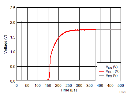
| VIN = 2.3 V | IOUT = 500 mA | COUT = 1 µF |
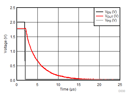
| VIN = 2.3 V | IOUT = 500 mA (3.6 Ω) | COUT = 1 µF |
10 Power Supply Recommendations
This device is designed to operate from an input supply voltage range of 1.6 V to 6.5 V. The input supply must be well regulated and free of spurious noise. To ensure that the LP5912-Q1 output voltage is well regulated and dynamic performance is optimum, the input supply must be at least VOUT + 0.5 V. A minimum capacitor value of 1 µF is required to be within 1 cm of the IN pin.
11 Layout
11.1 Layout Guidelines
The dynamic performance of the LP5912-Q1 is dependant on the layout of the PCB. PCB layout practices that are adequate for typical LDOs may degrade the PSRR, noise, or transient performance of the LP5912-Q1.
Best performance is achieved by placing CIN and COUT on the same side of the PCB as the LP5912-Q1, and as close to the package as is practical. The ground connections for CIN and COUT must be back to the LP5912-Q1 ground pin using as wide and as short of a copper trace as is practical.
Connections using long trace lengths, narrow trace widths, or connections through vias must be avoided. Such connections add parasitic inductances and resistance that result in inferior performance especially during transient conditions.
11.2 Layout Example
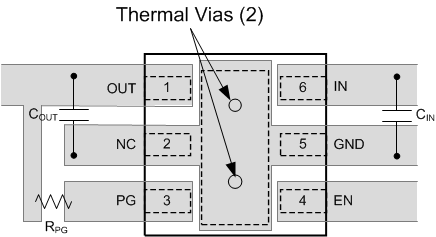 Figure 57. LP5912-Q1 Typical Layout