ZHCSEP0C October 2015 – February 2021 TPS61193
PRODUCTION DATA
- 1 特性
- 2 应用
- 3 说明
- 4 Revision History
- 5 Pin Configuration and Functions
-
6 Specifications
- 6.1 Absolute Maximum Ratings
- 6.2 ESD Ratings
- 6.3 Recommended Operating Conditions
- 6.4 Thermal Information
- 6.5 Electrical Characteristics (1) (1)
- 6.6 Internal LDO Electrical Characteristics
- 6.7 Protection Electrical Characteristics
- 6.8 Current Sinks Electrical Characteristics
- 6.9 PWM Brightness Control Electrical Characteristics
- 6.10 Boost and SEPIC Converter Characteristics
- 6.11 Logic Interface Characteristics
- 6.12 Typical Characteristics
- 7 Detailed Description
- 8 Application and Implementation
- 9 Power Supply Recommendations
- 10Layout
- 11Device and Documentation Support
- 12Mechanical, Packaging, and Orderable Information
7.4.1 Device States
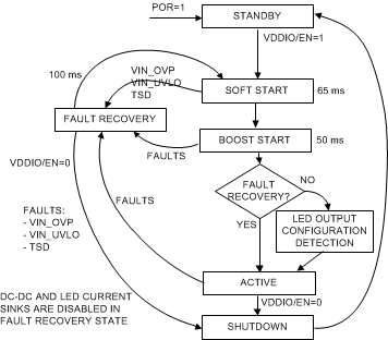
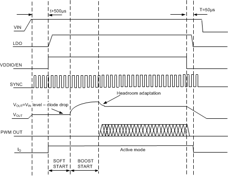
The TPS61193 enters STANDBY mode when the internal LDO output rises above the power-on reset level, VLDO > VPOR. In STANDBY mode the device is able to detect VDDIO/EN signal. When VDDIO/EN is pulled high, the device powers up. After start LED outputs are sensed to detect grounded outputs. Grounded outputs are disabled and excluded from the adaptive voltage control loop of the DC-DC. Please note that the input transient current would be maximum 1.2 mA while VDDIO/EN is powering up.
If a fault condition is detected, the device enters FAULT_RECOVERY state. Faults that cause the device to enter FAULT_RECOVERY are listed in Table 7-3. When LED open or short is detected, the faulty string is disabled, but device stays in ACTIVE mode.
 Figure 7-10 State Diagram
 Figure 7-11 Timing Diagram for the Typical Start-Up and Shutdown