-
AMC7834 具有温度、电流和电压监控功能的 12 位集成功率放大器监视和控制系统
- 1 特性
- 2 应用范围
- 3 说明
- 4 修订历史记录
- 5 Pin Configuration and Functions
-
6 Specifications
- 6.1 Absolute Maximum Ratings
- 6.2 ESD Ratings
- 6.3 Recommended Operating Conditions
- 6.4 Thermal Information
- 6.5 Electrical Characteristics—DAC Specifications
- 6.6 Electrical Characteristics—ADC, Current and Temperature Sensor Specifications
- 6.7 Electrical Characteristics—General Specifications
- 6.8 Serial Interface Timing Requirements
- 6.9 Switching Characteristics—DAC Specifications
- 6.10 Switching Characteristics—ADC, Current and Temperature Sensor Specifications
- 6.11 Switching Characteristics—General Specifications
- 6.12 Typical Characteristics
-
7 Detailed Description
- 7.1 Overview
- 7.2 Functional Block Diagram
- 7.3 Feature Description
- 7.4 Device Functional Modes
- 7.5 Programming
- 7.6
Register Maps
- 7.6.1 Power Mode: Address 0x02
- 7.6.2 Device Identification: Address 0x04 through 0x0C
- 7.6.3
General Device Configuration: Address 0x10 through 0x16
- 7.6.3.1 AMC Configuration 0 Register (address = 0x10) [reset = 0x0300]
- 7.6.3.2 AMC Configuration 1 Register (address = 0x11) [reset = 0x036A]
- 7.6.3.3 ADC MUX Register (address = 0x12) [reset = 0x0000]
- 7.6.3.4 Closed Loop Settling Time Register (address = 0x14) [reset = 0x2222]
- 7.6.3.5 DAC Sync Register (address = 0x15) [reset = 0x0000]
- 7.6.3.6 DAC Range Register (address = 0x16) [reset = 0x0000]
- 7.6.4
Clamp and Alarm Configuration: Address 0x17 through 0x1B
- 7.6.4.1 CLAMP Configuration Register (address = 0x17) [reset = 0x003F]
- 7.6.4.2 SLEEP1 Configuration Register (address = 0x18) [reset = 0xFF00]
- 7.6.4.3 SLEEP2 Configuration Register (address = 0x19) [reset = 0xFF00]
- 7.6.4.4 ALARMOUT Clamp Register (address = 0x1A) [reset = 0x0000]
- 7.6.4.5 ALARMOUT Configuration Register (address = 0x1B) [reset = 0x0000]
- 7.6.5 Conversion Trigger: Address 0x1C
- 7.6.6 Reset: Address 0x1D
- 7.6.7 Device Status: Address 0x1E and 0x1F
- 7.6.8
ADC Data: Address 0x20 through 0x2F
- 7.6.8.1 ADCn-Internal-Data Register (address = 0x20 to 0x23) [reset = 0x0000]
- 7.6.8.2 ADCn-External-Data Register (address = 0x24 to 0x27) [reset = 0x0000]
- 7.6.8.3 CSn-Data Register (address = 0x28 to 0x2B) [reset = 0x0000]
- 7.6.8.4 LT-Data Register (address = 0x2D) [reset = 0x0000]
- 7.6.8.5 RTn-Data Register (address = 0x2E to 0x2F) [reset = 0x0000]
- 7.6.9 DAC Data: Address 0x30 through 0x37
- 7.6.10 Closed-Loop Control: Address 0x38 through 0x3B
- 7.6.11
Alarm Threshold Configuration: Address 0x40 through 0x4F
- 7.6.11.1 ADCINTn/CSn-Upper-Threshold Register (address = 0x40, 0x42, 0x44 and 0x46) [reset = 0x0FFF]
- 7.6.11.2 ADCINTn/CSn-Lower-Threshold Register (address = 0x41, 0x43, 0x45 and 0x47) [reset = 0x0000]
- 7.6.11.3 TS-Upper-Threshold Register (address = 0x48, 0x4A and 0x4C) [reset = 0x07FF]
- 7.6.11.4 TS-Lower-Threshold Register (address = 0x49, 0x4B and 0x4D) [reset = 0x0800]
- 7.6.11.5 DACnn-Upper-Threshold Register (address = 0x4E and 0x4F) [reset = 0x0FFF]
- 7.6.12 Alarm Hysteresis Configuration: Address 0x50 and 0x56
- 7.6.13 GPIO: Address 0x58
- 8 Application and Implementation
- 9 Power Supply Recommendations
- 10Layout
- 11器件和文档支持
- 12机械、封装和可订购信息
- 重要声明
AMC7834 具有温度、电流和电压监控功能的 12 位集成功率放大器监视和控制系统
1 特性
- 8 个具有可编程范围的单调性 12 位数模转换器 (DAC)
- 4 个双极 DAC:
–4V 至 1V,–5V 至 0V 以及 0V 至 5V - 4 个单极 DAC:
0V 至 5V 以及 2.5V 至 7.5V - 高电流驱动能力:高达 ±10mA
- 可选钳位电压
- 4 个双极 DAC:
- 多通道 12 位逐次逼近寄存器 (SAR) 模数转换器 (ADC)
- 4 个外部模拟输入:0V 至 2.5V 范围
- 4 个用于双极 DAC 监视的内部输入
- 可编程超范围警报
- 4 个高侧电流感测放大器
- 共模电压:4V 至 60V
- 可选闭环漏极电流控制器操作
- 温度感测功能
- 内部温度传感器
- 2 个远程温度二极管驱动器
- 2.5V 内部基准电压
- 4 个通用 I/O 端口 (GPIO)
- 低功耗 SPI 兼容串行接口
- 4 线模式,1.7V 至 3.6V 工作电压
- 工作温度范围:-40°C 至 +125°C
- 采用 56 引脚超薄型四方扁平无引线 (VQFN) 封装
2 应用范围
- 通信基础设施:
- 蜂窝基站
- 微波回程
- 光纤网络
- 通用监视器和控制
- 数据采集系统
3 说明
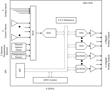
AMC7834 器件是一款针对功率放大器 (PA) 偏置的高度集成、低功耗、模拟监视和控制解决方案,能够对温度、电流和电压进行监控。
该器件集成了一个多通道 12 位模数转换器 (ADC);八个 12 位数模转换器 (DAC);四个高侧电流感测放大器,可以选择设置它们作为四个独立闭环漏极电流控制器的一部分;一个精确的片上温度传感器和两个远程温度二极管驱动器;四个可配置的通用 I/O 端口 (GPIO);以及一个精确的内部基准。其高集成度极大地减少了组件数量,并且简化了 PA 偏置系统设计。
该器件具有功能集成和宽工作温度范围等诸多优势,因此适合用作多通道射频 (RF) 通信系统中 PA 的一体化、低成本偏置控制电路。凭借灵活的 DAC 输出范围和宽共模电压电流传感器,此器件可用作针对多种晶体管技术(例如 LDMOS、GaA 和 GaN)的偏置解决方案。AMC7834 功能集对通用监视器和控制系统而言同样有益。
德州仪器 (TI) 提供 了一个完备的模拟监视和控制 (AMC) 产品系列, 以满足各类应用不同的通道数、附加特性或者转换器解决方案需求。更多信息,敬请访问 www.ti.com.cn/amc。
器件信息(1)
| 器件型号 | 封装 | 封装尺寸(标称值) |
|---|---|---|
| AMC7834 | VQFN (56) | 8.00mm x 8.00mm |
- 如需了解所有可用封装,请见数据表末尾的可订购产品附录。
4 修订历史记录
Changes from A Revision (April 2015) to B Revision
- deleted text from the Description of pin 1 in the Pin Functions table " If unused the pin requires a 10 kΩ pullup resistor to the IOVDD pin."Go
- Added: Bipolar DACs in AVSS clamp mode To the Clamp Output Mode section of Electrical Characteristics—DAC Specifications Go
- Deleted text from the Accuracy Test Conditions: "32 Samples Average" in Electrical Characteristics—ADC, Current and Temperature Sensor Specifications Go
- Added: AVDD alarm threshold to Electrical Characteristics—General Specifications Go
- Changed the IIOVDD (Power-Mode 10) TYP value From: 1 µA To 1.75 µA in Electrical Characteristics—General Specifications Go
- Changed the IIOVDD (Power-Mode 00) TYP value From: 0.2 µA To 1.75 µA in Electrical Characteristics—General SpecificationsGo
- Added Figure 29 Go
- Changed Figure 45Go
- Added text to the itemized list in DAC Clamp Operation: "If the output buffer is inactive the clamp voltage is fixed to AVSS."Go
- Added text to the end of DAC Clamp Operation: "Additionally, in the unique case..."Go
- Changed text in paragraph 1 of ADC Sequencing From: "The AMC7834 supports autonomous ADC conversion" To: The AMC7834 supports autonomous and direct-mode conversions..."Go
- Change the paragraph: "Once the conversion cycle starts..." in ADC SequencingGo
- Deleted text from paragraph 3 of ADC Sequencing: "The first conversion sequence is reserved for calibration and the corresponding ADC results should be ignored."Go
- Added text to the last paragraph of ADC Sequencing: "In direct-mode conversion the DAV/ADC_RDY pin ... for each channel group. "Go
- Added text to paragraph 3 of Drain Switch Control: The PA_ON signal state is also triggered by the AVDD monitoring circuitGo
- Changed text in two locations of paragraph 4 in Drain Switch Control: From: "AVSS" To: "AVDD and AVSS" Go
- Added text to the last paragraph of Drain Switch Control: "The AVDD detection circuit is set to trigger the PA_ON signal to the OFF state in response to an out of range event." Go
- Added section: AVDD Detection Alarm Go
- Changed text in the second paragraph of Open-Loop Mode From: "The current-sense amplifier outputs are converted continuously by the device ADC.." To: "The current-sense amplifier outputs are converted by the device ADC.." Go
- Changed 0x06 Default value From: 0000 To: 0001 in Table 9 Go
- Changed R-00h To: R-01h in Bits 7:0 of Figure 69 Go
- Changed the Reset value From: 0000h To: 0001h in Table 13 Go
- Changed Bit 12 of Table 15 From: Reserved To: CMODE Go
- Changed Bit 10 of Table 18 From: 000: Invalid To: 000: 1 Go
- Changed Bit 5-4 of Table 18 From: 00: Invalid To: 00: 1 Go
- Changed Bit 3-2 of Table 18 From: 00: Invalid To: 00: 1 Go
- Changed Bit 1-0 of Table 18 From: 00: Invalid To: 00: 1 Go
- Changed General Status Register (address = 0x1F) [reset = 0x0000]Go
- Added text to item 2 of Initialization Procedure: A 250 µs POR delay occurs..." Go
Changes from * Revision (November 2014) to A Revision
- 发布完整版量产数据数据表 Go
5 Pin Configuration and Functions
Pin Functions
| PIN | TYPE | DESCRIPTION | |
|---|---|---|---|
| NAME | NO. | ||
| ADC1 | 48 | I | Analog inputs channels. These channels are used for general monitoring. The input range of these pins is 0 to Vref. |
| ADC2 | 47 | I | |
| ADC3 | 46 | I | |
| ADC4 | 45 | I | |
| AGND1 | 17 | — | Analog ground. These pins are the ground reference point for all analog circuitry on the device. Connect the AGND1, AGND2, AGND3, and AGND4 pins to the same potential (AGND). Ideally, the analog and digital grounds should be at the same potential (GND) and must not differ by more than ±0.3 V. |
| AGND2 | 22 | — | |
| AGND3 | 35 | — | |
| AGND4 | 43 | — | |
| ALARMOUT | 2 | O | ALARMOUT is an open drain global alarm output. An external 10 kΩ pullup resistor to a voltage no higher than AVDD is required. The ALARMOUT output polarity is defined through the ALARMOUT-POLARITY bit in register 0x1B. The default polarity is active low. |
| AUXDAC1 | 15 | O | Auxiliary DAC Outputs. The power-on-reset and clamp voltage for these DACs is always AGND. |
| AUXDAC2 | 16 | O | |
| AUXDAC3 | 18 | O | |
| AUXDAC4 | 19 | O | |
| AVCC | 14 | — | Positive analog power supply for the auxiliary DACs. |
| AVDD1 | 26 | — | Analog supply voltage (4.5 V to 5.5 V). Connect the AVDD1 and AVDD2 pins to the same potential (AVDD). These pins must have the same value as the DVDD pin. |
| AVDD2 | 44 | — | |
| AVSS | 25 | — | Lowest potential in the system. This pin is typically tied to a negative supply voltage. If all the bipolar DACs are set to operate in positive output ranges can be connected to the analog ground. |
| CS | 8 | I | Active low serial data enable. This input is the frame synchronization signal for the serial data. When this signal goes low, it enables the serial interface input shift register. |
| D1+ | 52 | I | Remote temperature sensor D1. This pin is a positive input when D1 is enabled. This pin can be left unconnected if unused. |
| D1– | 51 | I | Remote temperature sensor D1. This pin is a negative input when D1 is enabled. This pin can be left unconnected if unused. Pins D1– and D2– are internally shorted. |
| D2+ | 50 | I | Remote temperature sensor D2. This pin is a positive input when D2 is enabled. This pin can be left unconnected if unused. |
| D2– | 49 | I | Remote temperature sensor D2. This pin is a negative input when D2 is enabled. This pin can be left unconnected if unused. Pins D1– and D2– are internally shorted. |
| DAC1 | 23 | O | Bipolar DAC outputs 1 and 2. These DACs share the same range and clamp voltage. |
| DAC2 | 24 | O | |
| DAC3 | 27 | O | Bipolar DAC outputs 3 and 4. These DACs share the same range and clamp voltage. |
| DAC4 | 28 | O | |
| DACTRIG | 6 | I | DAC trigger active low control input. When the DACTRIG pin is low, the contents of the DAC data registers are transferred to the DAC active registers. The DAC outputs update only after the DAC active registers have been loaded. This pin is only operational in open loop current sensing mode. |
| DAV/ADC_RDY | 1 | O | The DAV/ADC_RDY pin is in high-impedance mode by default and must be enabled through the DAVPIN-EN bit in register 0x11 to access the DAV or ADC_RDY functionality.
DAV is an active low ADC synchronization signal. A 20 µs pulse (active low) on this pin is used to indicate the end of a conversion sequence. Alternatively the pin can be set to operate as ADC_RDY through the DAVPIN-SEL bit in register 0x11. ADC_RDY is an active high synchronization signal used to indicate when the ADC is in the READY state. |
| DGND | 11 | — | Digital ground. This pin is the ground reference point for all digital circuitry on the device. Ideally, the analog and digital grounds should be at the same potential (GND) and must not differ by more than ±0.3 V. |
| DVDD | 13 | — | Digital supply voltage (4.5 V to 5.5 V). This pin must be the same value as the AVDD pins. |
| GPIO1 | 56 | I/O | General-purpose digital I/Os. These pins are bidirectional open-drain, digital I/Os and requires an external 10 kΩ pullup resistor to a voltage no higher than AVDD. If unused, the GPIO pins should be connected to ground. |
| GPIO2 | 55 | I/O | |
| GPIO3 | 54 | I/O | |
| GPIO4 | 53 | I/O | |
| IOVDD | 12 | — | IO supply voltage (1.7 V to 3.6 V). This pin sets the I/O operating voltage and threshold levels. |
| PAVDD | 41 | — | Power supply for the PA_ON control signal (4 V to 20 V). |
| PA_ON | 40 | O | PA_ON is a synchronization signal capable of driving an external PMOS switch and controlling the flow of drain current to a power amplifier (PA) transistor. The PA_ON pin has an internal 120 kΩ pull-up resistor to the PAVDD pin. The maximum output voltage is set by the PAVDD pin and limited to 20 V. For drain voltages higher than 20 V, tying the PAVDD pin to the AVDD pins and scaling the control signal externally is recommended. The PA_ON signal state can be set through a register write but it can also be configured to trigger automatically in the case of an ALARM event or when any of the SLEEP signals is activated. |
| REF_CMP | 42 | I/O | Reference compensation capacitor connection. Connect a 4.7 μF capacitor between this pin and the AGND4 pin for ADC reference compensation. |
| REF_IN | 20 | I | Reference input to the device. This pin can be connected to the REF_OUT pin to use the device internal reference or alternatively to an external voltage reference source. |
| REF_OUT | 21 | O | Internal voltage reference output. Connect this pin directly to the REF_IN pin to operate the device in internal reference mode. An external buffer amplifier with a high impedance input is required to drive an external load. This pin can be left unconnected. |
| RESET | 5 | I | Active low reset input. Logic low on this pin causes the device to perform a hardware reset. |
| SCLK | 7 | I | Serial interface clock. |
| SDI | 9 | I | Serial interface data input. Data is clocked into the input shift register on each rising edge of the SCLK pin. |
| SDO | 10 | O | Serial interface data output. The SDO pin is in high impedance when the CS pin is high. Data is clocked out of the input shift register on each falling edge of the SCLK pin. |
| SENSE1+ | 39 | I | Current sense 1 external sense resistor power connection |
| SENSE1– | 38 | I | Current sense 1 external sense resistor load connection |
| SENSE2+ | 37 | I | Current sense 2 external sense resistor power connection |
| SENSE2– | 36 | I | Current sense 2 external sense resistor load connection |
| SENSE3+ | 34 | I | Current sense 3 external sense resistor power connection |
| SENSE3– | 33 | I | Current sense 3 external sense resistor load connection |
| SENSE4+ | 32 | I | Current sense 4 external sense resistor power connection |
| SENSE4– | 31 | I | Current sense 4 external sense resistor load connection |
| SLEEP1 | 3 | I | Active high asynchronous power down digital input 1. The power down functions of this pin are register configurable. |
| SLEEP2 | 4 | I | Active high asynchronous power down digital input 2. The power down functions of this pin are register configurable. |
| VCLAMP1 | 30 | I | Power-on reset and clamp voltage control input for bipolar DACs 1 and 2. The resulting power-on reset (POR) and clamp voltage value is given by Equation 1. Equation 1. CLAMP = –3 × VCLAMP[1:2]
|
| VCLAMP2 | 29 | I | Power-on reset and clamp voltage control input for bipolar DACs 3 and 4. The resulting POR and clamp voltage value is given by Equation 1. |
| Thermal Pad | — | The thermal pad is located on the bottom-side of the device package. The thermal pad should be tied to the same potential as the AVSS pin for optimal thermal dissipation. Alternatively, the thermal pad can be left unconnected. | |
6 Specifications
6.1 Absolute Maximum Ratings
over operating free-air temperature range (unless otherwise noted)(1)| MIN | MAX | UNIT | ||
|---|---|---|---|---|
| Supply voltage | AVDD to GND | –0.3 | 6 | V |
| DVDD to GND | –0.3 | 6 | ||
| IOVDD to GND | –0.3 | 6 | ||
| AVCC to GND | –0.3 | 13 | ||
| AVSS to GND | –6 | 0.3 | ||
| PAVDD to AVSS | –0.3 | 26 | ||
| DGND to AGND | –0.3 | 0.3 | ||
| Pin voltage | ADC analog input voltage to GND | –0.3 | AVDD + 0.3 | V |
| Current sense input voltage to GND | –0.3 | 65 | ||
| Bipolar DAC outputs to GND | AVSS – 0.3 | AVDD + 0.3 | ||
| Auxiliary DAC outputs to GND | –0.3 | AVCC + 0.3 | ||
| VCLAMP1, VCLAMP2 inputs to GND | –0.3 | AVDD + 0.3 | ||
| D1+, D1–, D2+ and D2– to GND | –0.3 | AVDD + 0.3 | ||
| REF_CMP, REF_IN to GND | –0.3 | AVDD + 0.3 | ||
| REF_OUT to GND | –0.3 | AVDD + 0.3 | ||
| PA_ON to GND | –0.3 | PAVDD + 0.3 | ||
| CS, SCLK, SDI, DACTRIG, RESET, SLEEP1, SLEEP2 and DAV/ADC_RDY to GND | –0.3 | IOVDD + 0.3 | ||
| SDO to GND | –0.3 | IOVDD + 0.3 | ||
| GPIOs, ALARMOUT to GND | –0.3 | 6 | ||
| Pin current | ADC analog input current | –10 | 10 | mA |
| REF_OUT output current | –0.3 | 0.3 | ||
| GPIOs, ALARMOUT sinking current | 5 | |||
| Operating temperature range | –40 | 125 | °C | |
| Junction temperature range, TJ max | –40 | 150 | °C | |
| Storage temperature, Tstg | –40 | 150 | °C | |
6.2 ESD Ratings
| VALUE | UNIT | |||
|---|---|---|---|---|
| V(ESD) | Electrostatic discharge | Human body model (HBM), per ANSI/ESDA/JEDEC JS-001(1) | ±750 | V |
| Charged device model (CDM), per JEDEC specification JESD22-C101(2) | ±250 | |||
6.3 Recommended Operating Conditions
over operating free-air temperature range (unless otherwise noted)| MIN | NOM | MAX | UNIT | ||
|---|---|---|---|---|---|
| Supply voltage | AVDD(1) | 4.5 | 5 | 5.5 | V |
| DVDD(1) | 4.5 | 5 | 5.5 | ||
| IOVDD | 1.7 | 3.3 | 3.6 | ||
| AVCC | 4.5 | 5 | 12.5 | ||
| AVSS(2) | –5.5 | –5 | 0 | ||
| PAVDD | 4 | 5 | 20 | ||
| Specified performance temperature | –40 | 25 | 105 | °C | |
| Operating temperature | –40 | 25 | 125 | °C | |
6.4 Thermal Information
| THERMAL METRIC(1)(2) | RTQ (VQFN) | UNIT | |
|---|---|---|---|
| 56 PINS | |||
| RθJA | Junction-to-ambient thermal resistance | 24.7 | °C/W |
| RθJC(top) | Junction-to-case (top) thermal resistance | 7.9 | |
| RθJB | Junction-to-board thermal resistance | 2.7 | |
| ψJT | Junction-to-top characterization parameter | 0.2 | |
| ψJB | Junction-to-board characterization parameter | 2.7 | |
| RθJC(bot) | Junction-to-case (bottom) thermal resistance | 0.3 | |
6.5 Electrical Characteristics—DAC Specifications
The electrical ratings specified in this section apply to all specifications in this document, unless otherwise noted. These specifications are interpreted as conditions that do not degrade the device parametric or functional specifications for the life of the product containing it. AVDD = DVDD = 5 V, AVCC = 5 V, AVSS = –5 V, IOVDD = 3.3 V, PAVDD = 5 V, AGND = DGND = 0 V, external 2.5 V reference, DAC output range = 0 to 5 V for all DACs, no load on the DACs, current sense inputs common mode at 48 V, TA = –40°C to +105°C| PARAMETER | TEST CONDITIONS | MIN | TYP | MAX | UNIT | |
|---|---|---|---|---|---|---|
| BIPOLAR DAC DC ACCURACY | ||||||
| Resolution | 12 | Bits | ||||
| INL | Relative accuracy | Measured by line passing through codes 040h and FC0h. 0 to 5 V range | ±0.3 | ±1 | LSB | |
| Measured by line passing through codes 040h and FC0h. –4 to 1 V and –5 to 0 V ranges | ±0.3 | ±1 | ||||
| DNL | Differential nonlinearity | Specified monotonic. Measured by line passing through codes 040h and FC0h. 0 to 5 V range | ±0.05 | ±1 | LSB | |
| Specified monotonic. Measured by line passing through codes 040h and FC0h. –4 to 1 V and –5 to 0 V ranges | ±0.05 | ±1 | ||||
| TUE | Total unadjusted error | TA = 25°C, 0 to 5 V range | ±1 | ±15 | mV | |
| TA = 25°C, –4 to 1 V and –5 to 0 V ranges | ±2 | ±15 | ||||
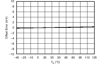
| Offset error | TA = 25°C. Measured by line passing through codes 040h and FC0h. 0 to 5 V range | ±0.2 | ±10 | mV | ||
| Zero-code error | TA = 25°C. Code 000h. –4 to 1 V and –5 to 0 V ranges. AVSS = –5.5 V | ±2 | ±10 | mV | ||
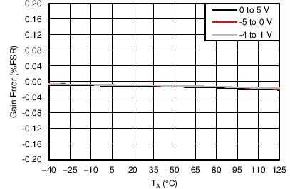
| Gain error | TA = 25°C. Measured by line passing through codes 040h and FC0h. 0 to 5 V range | ±0.02 | ±0.2 | %FSR | ||
| TA = 25°C. Measured by line passing through codes 040h and FC0h. –4 to 1 V and –5 to 0 V ranges | ±0.02 | ±0.2 | ||||
| Offset temperature drift | 0 to 5 V range | ±1 | ppm/°C | |||
| Zero-code temperature drift | –4 to 1 V and –5 to 0 V ranges. AVSS = –5.5 V | ±1.5 | ppm/°C | |||
| Gain temperature drift | All output ranges | ±1 | ppm/°C | |||
| AUXILIARY DAC DC ACCURACY | ||||||
| Resolution | 12 | Bits | ||||
| INL | Integral nonlinearity | Measured by line passing through codes 040h and FC0h. 0 to 5 V range | ±0.5 | ±1.25 | LSB | |
| Measured by line passing through codes 040h and FC0h. 2.5 to 7.5 V range. AVCC = 12 V | ±0.5 | ±1.25 | ||||
| DNL | Differential nonlinearity | Specified monotonic. Measured by line passing through codes 040h and FC0h. 0 to 5 V range | ±0.05 | ±1 | LSB | |
| Specified monotonic. Measured by line passing through codes 040h and FC0h. 2.5 to 7.5 V range. AVCC = 12 V | ±0.05 | ±1 | ||||
| TUE | Total unadjusted error | TA = 25°C. 0 to 5 V range | ±2 | ±15 | mV | |
| TA = 25°C. 2.5 to 7.5 V range. AVCC = 12 V | ±2 | ±15 | ||||
| Offset error | TA = 25°C. Measured by line passing through codes 040h and FC0h. 0 to 5 V range | ±0.3 | ±10 | mV | ||
| TA = 25°C. Measured by line passing through codes 040h and FC0h. 2.5 to 7.5 V range. AVCC = 12 V | ±1 | ±10 | ||||
| Gain error | TA = 25°C. Measured by line passing through codes 040h and FC0h. 0 to 5 V range | ±0.03 | ±0.2 | %FSR | ||
| TA = 25°C. Measured by line passing through codes 040h and FC0h. 2.5 to 7.5 V range. AVCC = 12 V | ±0.03 | ±0.2 | ||||
| Offset temperature drift | All output ranges | ±1 | ppm/°C | |||
| Gain temperature drift | All output ranges | ±1 | ppm/°C | |||
| DAC OUTPUT CHARACTERISTICS | ||||||
| Bipolar DAC range(1) | DACn_range set to 00 | –4 | 1 | V | ||
| DACn_range set to 01 | –5 | 0 | ||||
| DACn_range set to 10 | –5 | 0 | ||||
| DACn_range set to 11 | 0 | 5 | ||||
| Auxiliary DAC range(2) | AUXDACn_range set to 0 | 0 | 5 | V | ||
| AUXDACn_range set to 1 | 2.5 | 7.5 | ||||
| Short-circuit current | Bipolar DACs: Full-scale current shorted to AVSS or AVDD
Auxiliary DACs: Full-scale current shorted to AGND or AVCC |
45 | mA | |||
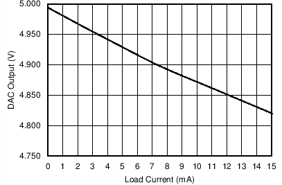
| Load current(3) | Bipolar DACs: Source or sink with 300 mV headroom from AVDD or AVSS, voltage drop < 25 mV Auxiliary DACs: Source or sink with 300 mV headroom from AVCC or AGND, voltage drop < 25 mV |
±10 | mA | |||
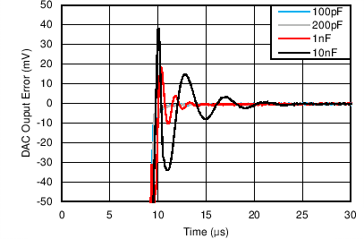
| Maximum capacitive load(4) | All DAC outputs. RL = ∞ | 0 | 10 | nF | ||
| DC output impedance | All DAC outputs. Code set to 800h, ±10 mA | 1 | Ω | |||
| Glitch energy | All DAC outputs. Transition: Code 7FFh to 800h; 800h to 7FFh | 1 | nV-s | |||
| Output noise | Auxiliary DACs. 1 kHz, code 800h | 200 | nV/√Hz | |||
| Bipolar DACs. 1 kHz, code 800h | 100 | |||||
| Auxiliary DACs. Integrated noise from 0.1 Hz to 10 Hz, code 800h | 20 | µVPP | ||||
| Bipolar DACs. Integrated noise from 0.1 Hz to 10 Hz, code 800h | 10 | |||||
| CLAMP OUTPUT MODE | ||||||
| VCLAMP [1:2] voltage range | 0 | –AVSS / 3 | V | |||
| VCLAMP [1:2] input current | ±0.5 | µA | ||||
| Clamp output voltage | Bipolar DACs. Clamp voltage = –3 × VCLAMP[1:2] | AVSS | 0 | V | ||
| Auxiliary DACs | AGND | |||||
| Clamp output current | Bipolar DACs. Source, sink, or both with 300-mV headroom from AVSS, voltage drop < 25 mV | ±10 | mA | |||
| Clamp pull-down resistance | Auxiliary DACs. Measured to AGND | 9 | kΩ | |||
| Bipolar DACs. VCLAMP buffers inactive (AVSS clamp mode). Measured to AVSS | 550 | Ω | ||||
6.6 Electrical Characteristics—ADC, Current and Temperature Sensor Specifications
The electrical ratings specified in this section apply to all specifications in this document, unless otherwise noted. These specifications are interpreted as conditions that do not degrade the device parametric or functional specifications for the life of the product containing it. AVDD = DVDD = 5 V, AVCC = 5 V, AVSS = –5 V, IOVDD = 1.8 to 3.3 V, PAVDD = 5 V, AGND = DGND = 0 V, external 2.5 V reference, DAC output range = 0 to 5 V for all DACs, no load on the DACs, current sense inputs common mode at 48 V, TA = –40°C to +105°C| PARAMETER | TEST CONDITIONS | MIN | TYP | MAX | UNIT | |
|---|---|---|---|---|---|---|
| EXTERNAL ANALOG INPUTS (ADC1, ADC2, ADC3 and ADC4) | ||||||
| Resolution | 12 | Bits | ||||
| INL | Integral nonlinearity | ±0.5 | ±1 | LSB | ||
| DNL | Differential nonlinearity | Specified monotonic | ±0.5 | ±1 | LSB | |
| Offset error | ±0.3 | ±4.5 | LSB | |||
| Offset error match | ±1 | LSB | ||||
| Gain error | ±0.3 | ±4 | LSB | |||
| Gain error match | ±1 | LSB | ||||
| Full-scale input range(1) | 0 | Vref | V | |||
| Input capacitance | 48 | pF | ||||
| DC-input leakage current | Unselected ADC input | ±2 | µA | |||
| INTERNAL MONITORING INPUTS (BIPOLAR DAC-OUTPUT MONITORING) | ||||||
| Full scale input range(1) | –5 | 2.5 | V | |||
| Resolution | LSB size | 1.83 | mV | |||
| CURRENT-SENSE INPUTS | ||||||
| Common mode voltage | 4 | 60 | V | |||
| Full scale sense voltage(1) | SENSEn+ – SENSEn- | 0 | 200 | mV | ||
| Input resistance | Per current sense input terminal | 192 | kΩ | |||
| Gain accuracy | ±0.1% | ±1% | ||||
| Input offset error | CS-FILTER[2:0] = 100 Common mode voltage = 4 V |
±50 | ±500 | µV | ||
| CMRR | CS-FILTER[2:0] = 100 | 80 | dB | |||
| Resolution | LSB size | 48.83 | µV | |||
| TEMPERATURE SENSOR: INTERNAL | ||||||
| Operating range(1)(2) | Specified monotonic over entire range. | –55 | 125 | °C | ||
| Accuracy(2) | TJ = –40°C to 125°C | ±3 | °C | |||
| Resolution | LSB size TJ = –40°C to 125°C |
0.25 | °C | |||
| TEMPERATURE SENSOR: EXTERNAL (USING 2N3906 EXTERNAL TRANSISTOR) | ||||||
| Operating range(1)(2) | –55 | 150 | °C | |||
| Accuracy(2) | RT-SET[2:0] = 011, CS-FILTER[2:0] = 100 TA = –40°C to 125°C, T(DIODE) = –40°C to 150°C |
±3 | °C | |||
| Resolution | LSB size TA = –40°C to 125°C, T(DIODE) = –40°C to 150°C |
0.25 | °C | |||
6.7 Electrical Characteristics—General Specifications
The electrical ratings specified in this section apply to all specifications in this document, unless otherwise noted. These specifications are interpreted as conditions that do not degrade the device parametric or functional specifications for the life of the product containing it. AVDD = DVDD = 5 V, AVCC = 5 V, AVSS = –5 V, IOVDD = 1.8 to 3.3 V, PAVDD = 5 V, AGND = DGND = 0 V, external 2.5 V reference, DAC output range = 0 to 5 V for all DACs, no load on the DACs, current sense inputs common mode at 48 V, TA = –40°C to 105°C| PARAMETER | TEST CONDITIONS | MIN | TYP | MAX | UNIT | |
|---|---|---|---|---|---|---|
| EXTERNAL REFERENCE INPUT | ||||||
| VREF_IN | Input voltage range | REF_IN pin | 2.5 | V | ||
| Input current | VREF_IN = 2.5 V | 1 | 100 | µA | ||
| DAC reference buffer offset | TA = 25°C | ±5 | mV | |||
| ADC reference buffer offset | TA = 25°C | ±5 | mV | |||
| INTERNAL REFERENCE | ||||||
| Output voltage | TA = 25°C, REF_OUT pin | 2.4925 | 2.5 | 2.5075 | V | |
| Reference temperature coefficient | 10 | 35 | ppm/°C | |||
| Output voltage noise | 1 kHz | 260 | nV/√Hz | |||
| Integrated noise from 0.1 Hz to 10 Hz | 13 | µVPP | ||||
| PA_ON OUTPUT | ||||||
| PA_ON output voltage | PAVDD ≤ 20 V | AGND | PAVDD | V | ||
| SUPPLY ALARMS(1) | ||||||
| AVSS alarm threshold | –4.4 | –4.1 | –3.8 | V | ||
| AVDD alarm threshold | 3.4 | 3.9 | 4.4 | V | ||
| DIGITAL LOGIC(1) | ||||||
| VIH | High-level input voltage | IOVDD = 1.7 V to 3.6 V | 0.7 × IOVDD | V | ||
| VIL | Low-level input voltage | IOVDD = 1.7 V to 3.6 V | 0.3 × IOVDD | V | ||
| Vhys | Hysteresis voltage | IOVDD = 1.7 V to 3.6 V | 0.1 × IOVDD | V | ||
| VOH | High-level output voltage | SDO and DAV/ADC_RDY. IOVDD = 1.7 V, I(LOAD) = 1 mA | IOVDD – 0.4 | V | ||
| VOL | Low-level output voltage | IOVDD = 1.7 V to 3.6 V, I(LOAD) = –1 mA | 0.4 | V | ||
| High impedance leakage | ±0.5 | µA | ||||
| High impedance output capacitance | 10 | pF | ||||
| POWER REQUIREMENTS | ||||||
| IAVDD | AVDD supply current | POWER-MODE = 10. AVDD = DVDD = 5.5 V, AVCC = 5.5 V PAVDD = 20 V, AVSS = –5.5 V, IOVDD = 3.6 V All monitoring channels enabled Bipolar DACs in –5 to 0 V range Auxiliary DACs in 0 to 5 V range All DACs at 800h code. PA_ON in "ON" state |
10 | 12.5 | mA | |
| IAVCC | AVCC supply current | 1.5 | 2 | mA | ||
| IAVSS | AVSS supply current | –3.5 | –2.5 | mA | ||
| IDVDD | DVDD supply current | 2.5 | 3 | mA | ||
| IIOVDD | IOVDD supply current | 1.75 | 2.5 | µA | ||
| IPAVDD | PAVDD supply current | 170 | 250 | µA | ||
| Power consumption | 95 | 120.5 | mW | |||
| IAVDD | AVDD supply current | POWER-MODE = 00. AVDD = DVDD = 5.5 V, AVCC = 5.5 V PAVDD = 20 V, AVSS = –5.5 V, IOVDD = 3.6 V All DACs in clamp mode at 0 V PA_ON in "OFF" state |
3.5 | mA | ||
| IAVCC | AVCC supply current | 0.2 | mA | |||
| IAVSS | AVSS supply current | –2 | mA | |||
| IDVDD | DVDD supply current | 2.5 | mA | |||
| IIOVDD | IOVDD supply current | 1.75 | µA | |||
| IPAVDD | PAVDD supply current | 12 | µA | |||
| Power consumption | 45 | mW | ||||
6.8 Serial Interface Timing Requirements(1)(2)
AVDD = DVDD = 5 V, AVCC = 5 V, AVSS = –5 V, PAVDD = 5 V, AGND = DGND = 0 V, external 2.5 V reference, DAC output range = 0 to 5 V for all DACs, no load on the DACs, current sense inputs common mode at 48 V, TA = –40°C to +105°C (unless otherwise noted)| IOVDD = 1.7 TO 2.7 V | IOVDD = 2.7 TO 3.6 V | UNIT | |||||
|---|---|---|---|---|---|---|---|
| MIN | MAX | MIN | MAX | ||||
| fSCLK | SCLK frequency | 0.2 | 10 | 0.2 | 15 | MHz | |
| tp | SCLK period | See Figure 1 and Figure 2. | 100 | 66.67 | ns | ||
| tPH | SCLK pulse width high | 40 | 26 | ns | |||
| tPL | SCLK pulse width low | 40 | 26 | ns | |||
| tsu | SDI setup | 10 | 10 | ns | |||
| th | SDI hold | 10 | 10 | ns | |||
| t(ODZ) | SDO driven to tri-state | See Figure 2. | 0 | 15 | 0 | 10 | ns |
| t(OZD) | SDO tri-state to driven | 0 | 20 | 0 | 15 | ns | |
| t(OD) | SDO output delay | 0 | 20 | 0 | 15 | ns | |
| tsu(CS) | CS setup | See Figure 1 and Figure 2 | 5 | 5 | ns | ||
| th(CS) | CS hold | 20 | 20 | ns | |||
| t(IAG) | Inter-access gap | 15 | 15 | ns | |||
6.9 Switching Characteristics—DAC Specifications
The electrical ratings specified in this section apply to all specifications in this document, unless otherwise noted. These specifications are interpreted as conditions that do not degrade the device parametric or functional specifications for the life of the product containing it. AVDD = DVDD = 5 V, AVCC = 5 V, AVSS = –5 V, IOVDD = 3.3 V, PAVDD = 5 V, AGND = DGND = 0 V, external 2.5 V reference, DAC output range = 0 to 5 V for all DACs, no load on the DACs, current sense inputs common mode at 48 V, TA = –40°C to +105°C| PARAMETER | TEST CONDITIONS | MIN | TYP | MAX | UNIT | |
|---|---|---|---|---|---|---|
| DAC OUTPUT CHARACTERISTICS | ||||||
| Output voltage settling time | Transition: Code 400h to C00h to within ½ LSB. RL= 2 kΩ, CL = 200 pF. All DAC outputs. All output ranges |
10 | µs | |||
| Slew rate | Transition: Code 400h to C00h, 10% to 90%. RL= 2 kΩ, CL = 200 pF. All DAC outputs. All output ranges |
1.25 | V/µs | |||
| CLAMP OUTPUT MODE | ||||||
| Clamp shutdown delay(1) | All DAC outputs. RL = ∞, CL = 200 pF, clamp from 3.5 V output, within 10% accuracy of active DAC output, measured from SLEEP 0 to 1 transition | 5 | µs | |||
| Wake-up from clamp delay(1) | All DAC outputs. RL = ∞, CL = 200 pF, wake-up to 3.5 V output, within 10% accuracy of active DAC output, measured from SLEEP 1 to 0 transition | 5 | µs | |||
6.10 Switching Characteristics—ADC, Current and Temperature Sensor Specifications
The electrical ratings specified in this section apply to all specifications in this document, unless otherwise noted. These specifications are interpreted as conditions that do not degrade the device parametric or functional specifications for the life of the product containing it. AVDD = DVDD = 5 V, AVCC = 5 V, AVSS = –5 V, IOVDD = 1.8 to 3.3 V, PAVDD = 5 V, AGND = DGND = 0 V, external 2.5 V reference, DAC output range = 0 to 5 V for all DACs, no load on the DACs, current sense inputs common mode at 48 V, TA = –40°C to +105°C| PARAMETER | TEST CONDITIONS | MIN | TYP | MAX | UNIT | |
|---|---|---|---|---|---|---|
| ADC INTERNAL OSCILLATOR | ||||||
| Internal oscillator frequency | 3.7 | 4 | 4.3 | MHz | ||
| EXTERNAL ANALOG INPUTS (ADC1, ADC2, ADC3 and ADC4) | ||||||
| Update time | All four external inputs enabled Internal monitoring inputs disabled |
1 | ms | |||
| INTERNAL MONITORING INPUTS (BIPOLAR DAC-OUTPUT MONITORING) | ||||||
| Update time | All four internal monitoring inputs enabled External analog inputs disabled |
1 | ms | |||
| CURRENT-SENSE INPUTS | ||||||
| Update time | All four current sense inputs enabled CS-FILTER[2:0] = 000 |
200 | µs | |||
| TEMPERATURE SENSOR: INTERNAL | ||||||
| Update time | Remote temperature sensors disabled | 2 | ms | |||
| TEMPERATURE SENSOR: EXTERNAL (USING 2N3906 EXTERNAL TRANSISTOR) | ||||||
| Update time | Single external temperature sensor Internal temperature sensor disabled RT-SET[2:0] = 000 |
8 | ms | |||
6.11 Switching Characteristics—General Specifications
The electrical ratings specified in this section apply to all specifications in this document, unless otherwise noted. These specifications are interpreted as conditions that do not degrade the device parametric or functional specifications for the life of the product containing it. AVDD = DVDD = 5 V, AVCC = 5 V, AVSS = –5 V, IOVDD = 1.8 to 3.3 V, PAVDD = 5 V, AGND = DGND = 0 V, external 2.5 V reference, DAC output range = 0 to 5 V for all DACs, no load on the DACs, current sense inputs common mode at 48 V, TA = –40°C to 105°C| PARAMETER | TEST CONDITIONS | MIN | TYP | MAX | UNIT | |
|---|---|---|---|---|---|---|
| PA_ON OUTPUT(1) | ||||||
| PA_ON OFF state enable | Measured from AVSS alarm event, CL = 1 nF | 1 | ms | |||
| Measured from SLEEP 0 to 1 transition, CL = 1 nF | 1 | ms | ||||
| PA_ON ON state enable | Measured from SLEEP 1 to 0 transition, CL = 1 nF | 0.5 | ms | |||
| RESET REQUIREMENTS(1) | ||||||
| Reset delay | Delay to normal operation from hardware reset | 100 | 250 | µs | ||
| Delay to normal operation from software reset | 10 | µs | ||||
| Reset pulse width | 20 | ns | ||||
 Figure 1. Serial Interface Write Timing Diagram
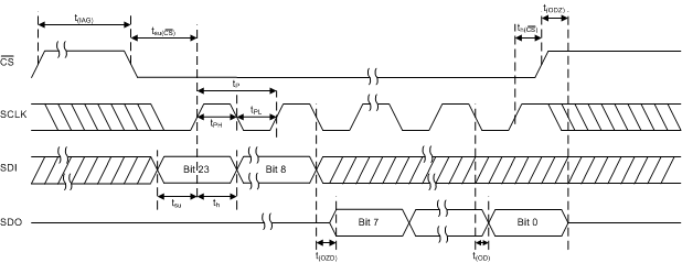 Figure 2. Serial Interface Read Timing Diagram
6.12 Typical Characteristics
6.12.1 Typical Characteristics: DAC
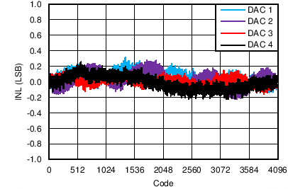
| DAC range = 0 to 5 V, AVDD = 5.5 V |
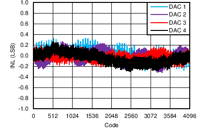
| DAC range = –5 to 0 V, AVSS = –5.5 V |
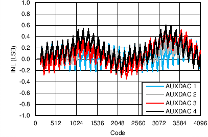
| DAC range = 0 to 5 V, AVCC = 5.5 V |
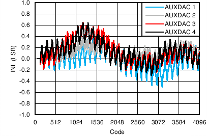
| DAC range = 2.5 to 7.5 V, AVCC = 12 V |
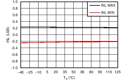
| DAC range = 0 to 5 V, AVDD = 5.5 V |
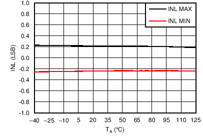
| DAC range = –5 to 0 V, AVSS = –5.5 V |
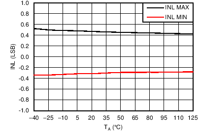
| DAC range = 0 to 5 V, AVCC = 5.5 V |
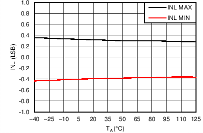
| DAC range = 2.5 to 7.5 V, AVCC = 12 V |
| DAC range = 0 to 5 V |
| AVDD = 5.5 V, AVSS = –5.5 V |
| DAC range = 0 to 5 V, Code 0xFFF |
| Code 0x000 to 0xFFF to within 0.5% of final value |
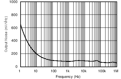
| Bipolar DAC, Code 0x800 |
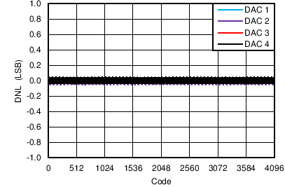
| DAC range = 0 to 5 V, AVDD = 5.5 V |
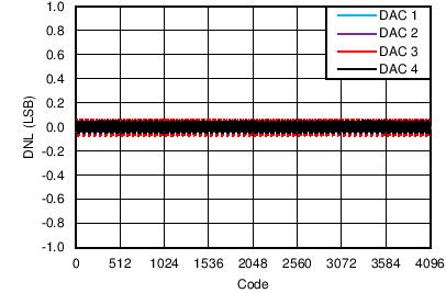
| DAC range = –5 to 0 V, AVSS = –5.5 V |
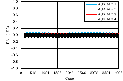
| DAC range = 0 to 5 V, AVCC = 5.5 V |
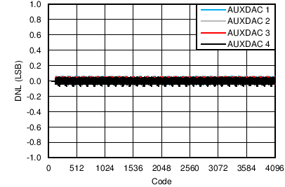
| DAC range = 2.5 to 7.5 V, AVCC = 12 V |
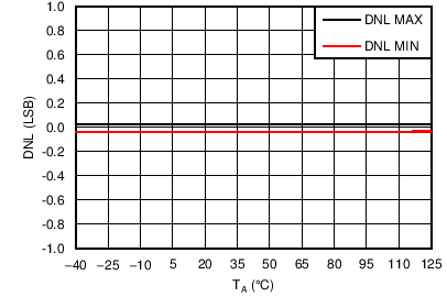
| DAC range = 0 to 5 V, AVDD = 5.5 V |
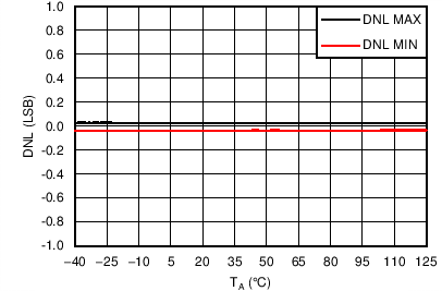
| DAC range = –5 to 0 V, AVSS = –5.5 V |
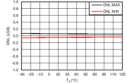
| DAC range = 0 to 5 V, AVCC = 5.5 V |
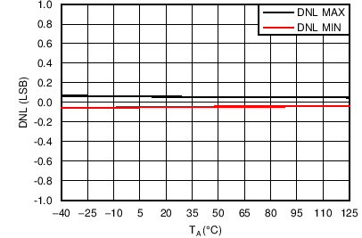
| DAC range = 2.5 to 7.5 V, AVCC = 12 V |
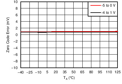
| AVSS = –5.5 V |
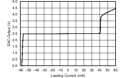
| DAC range = 0 to 5 V, Code 0x800 |
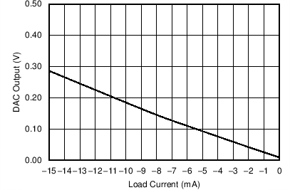
| DAC range = 0 to 5 V, Code 0x000, AVSS = 0 V |
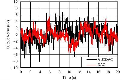
| Code 0x800 |
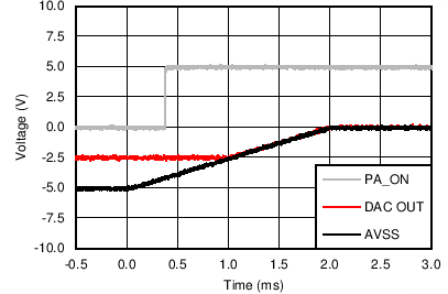
| DAC range: –5 to 0 V, Code 0x800 |
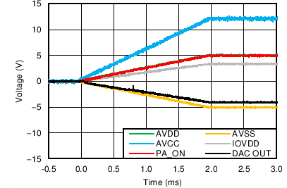
| DAC range: –4 to 1 V, VCLAMP[1:2] = 4/3 V |
6.12.2 Typical Characteristics: ADC
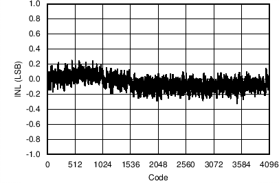
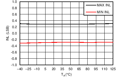
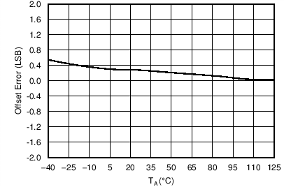
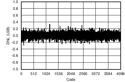
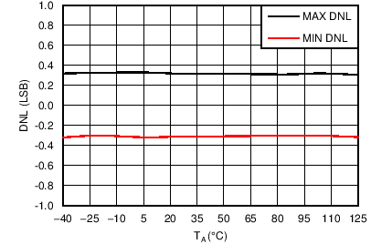
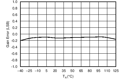
6.12.3 Typical Characteristics: Current Sense
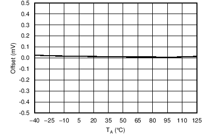
| VCM = 28 V, VSENSE = 0 V, CS-FILTER[2:0] = 100 |
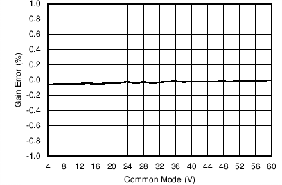
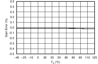
| VCM = 28 V |
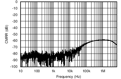
| CS-FILTER[2:0] = 100 |
6.12.4 Typical Characteristics: Temperature Sensor
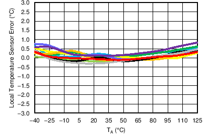
| 10 units |
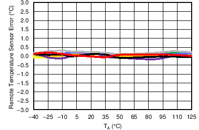
| 10 units, T(DIODE) = 25°C, RT-SET[2:0] = 011 |
6.12.5 Typical Characteristics: Reference
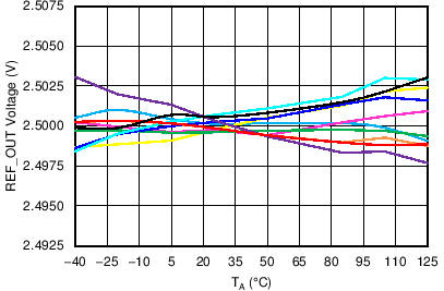
| 10 units |
7 Detailed Description
7.1 Overview
The AMC7834 is a highly-integrated analog-monitoring and control solution for power-amplifier (PA) biasing capable of current, temperature, and voltage supervision. The AMC7834 integrates the following features:
- Eight, 12-bit digital-to-analog converters (DACs) with programmable output ranges
- Four bipolar DACs with selectable output ranges: –4 to 1 V, –5 to 0 V, and 0 to 5 V
- The clamp and power-on-reset (POR) voltage for these DACs is pin-configurable.
- Four auxiliary DACs with selectable output ranges: 0 to 5 V and 2.5 to 7.5 V
- The clamp and POR voltage for these DACs is fixed to AGND.
- The DACs can be configured to clamp automatically upon detection of an alarm event.
- Four bipolar DACs with selectable output ranges: –4 to 1 V, –5 to 0 V, and 0 to 5 V
- A multi-channel, 12-bit analog-to-digital converter (ADC) for voltage, temperature, and current sensing
- Four external analog inputs: 0 to 2.5 V
- Four internal inputs for monitoring the bipolar DAC outputs
- Programmable threshold detectors
- Four high-side current-sense amplifiers
- Common mode voltages from 4 V up to 60 V
- The current sensors can optionally be set to operate as part of four independent closed-loop drain-current controllers
- Temperature sensing capabilities
- On-chip temperature sensor
- Two remote temperature sensor diode drivers
- Four general-purpose I/O (GPIO) ports
- Internal 2.5 V precision reference
- The device can operate from an internal reference. Alternatively an external reference can be used.
- Four-wire SPI-compatible interface supporting 1.7 to 3.6 V operation
The AMC7834 device is characterized for operation over the temperature range of –40ºC to 125ºC which makes the device suitable for harsh-condition applications. The device is available in an 8-mm × 8-mm 56-pin VQFN PowerPAD package.
The AMC7834 high-integration makes it an ideal all-in-one, low-cost, bias-control circuit for the PAs found in multi-channel RF communication systems. The flexible DAC output ranges allow the device to be used as a biasing solution for a large variety of transistor technologies such as LDMOS, GaAs, and GaN. The AMC7834 feature set is similarly beneficial in general-purpose monitor and control systems.
7.2 Functional Block Diagram
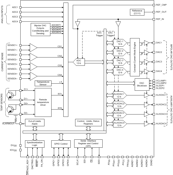
7.3 Feature Description
7.3.1 Digital-to-Analog Converters (DACs)
The AMC7834 device features an analog-control system centered on eight, 12-bit DACs that can operate from an external reference or the device internal reference. Each DAC core consists of a string DAC and an output-voltage buffer.
The resistor-string structure consists of a series of resistors, each with a value of R. The code loaded to the DAC determines at which node on the string the voltage is tapped off to be fed into the output amplifier. The voltage is tapped off by closing one of the switches connecting the string to the amplifier (see Figure 44). The resistor string architecture has inherent monotonicity, voltage output, and low glitch. The resistor string architecture is also linear because all the resistors are of equal value.
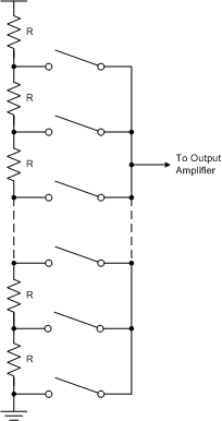 Figure 44. DAC Resistor String
7.3.1.1 DAC Configuration
The eight DACs are split into bipolar and auxiliary outputs based on their output range and clamping capabilities as listed in Table 1. After power-on or a reset event the DAC outputs are directed automatically to the corresponding clamp value and all DAC buffer and active registers are set to the default values.
Table 1. DAC Group Configuration
| DAC | TYPE | OUTPUT RANGES | CLAMP VOLTAGE | POWER SUPPLY RANGE | CLOSED LOOP OPERATION CAPABLE? |
|---|---|---|---|---|---|
| DAC1 and DAC2 | Bipolar | 0 to 5 V –4 to 1 V –5 to 0 V |
–3 × VCLAMP1 or AVSS | AVSS to AVDD | Yes |
| DAC3 and DAC4 | –3 × VCLAMP2 or AVSS | ||||
| AUXDAC1 | Auxiliary | 0 to 5 V 2.5 to 7.5 V |
AGND | AGND to AVCC | No |
| AUXDAC2 | |||||
| AUXDAC3 | |||||
| AUXDAC4 |
7.3.1.1.1 Bipolar DACs (DAC1, DAC2, DAC3, and DAC4)
The bipolar DACs are configured as DAC pairs (DAC1-DAC2 and DAC3-DAC4). The output range for each bipolar DAC pair can be configured through the DAC Range register (address 0x16) to one of the following: 0 to 5 V, –5 to 0 V, or –4 to 1 V. The POR and clamp value of each DAC pair is set by the pins VCLAMP1 (for the DAC1-DAC2 pair) and VCLAMP2 (for the DAC3-DAC4 pair) to any voltage between AVSS and 0 V during normal operation. If AVDD falls outside the device specified operating range the bipolar DACs enter the special AVSS clamp mode and their outputs are set to AVSS. The full-scale output range of the bipolar DACs is limited by the power supplies, AVDD and AVSS.
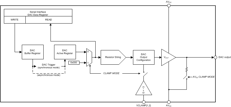
The bipolar DACs operate as standalone DACs when the AMC7834 is set in open-loop mode (LOOP-EN bit set to 0 in register 0x10). Figure 45 shows a high level block diagram of each bipolar DAC when operating in open-loop mode.
Alternatively, with the AMC7834 set in closed-loop mode (LOOP-EN bit set to 1 in register 0x10) each bipolar DAC output updates automatically in response to one of the four current sensors in the device (see the Closed-Loop Mode section). In closed-loop mode the AMC7834 bipolar DACs operate as four autonomous closed-loop current controllers.
The DAC upper threshold registers (address 0x4E through 0x4F) sets an upper output limit other than full-scale for the bipolar DACs when operating in closed-loop mode. The upper threshold feature can be used to limit the maximum output voltage for each bipolar DAC. When a closed-loop controller attempts to set its bipolar DAC to a value exceeding the corresponding DAC upper threshold register, the DAC is updated with the threshold code instead.
7.3.1.1.2 Auxiliary DACs (AUXDAC1, AUXDAC2, AUXDAC3, and AUXDAC4)
The output range for each auxiliary DAC can be independently set through the DAC Range register (address 0x16) to either 0 to 5 V or 2.5 to 7.5 V. The POR and clamp value of each of the auxiliary DACs is fixed to AGND. The maximum and minimum outputs from these DACs cannot exceed AVCC or be lower than AGND, respectively. Figure 46 shows a high level block diagram of each auxiliary DAC.
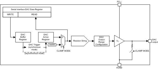 Figure 46. Auxiliary DAC Block Diagram
7.3.1.2 DAC Register Structure
The input data of the DACs is written to the individual DAC data registers (address 0x30 through 0x37) in straight binary format for all output ranges (see Table 2).
Table 2. DAC Data Format
| DIGITAL CODE | DAC OUTPUT VOLTAGE (V) | |||
|---|---|---|---|---|
| 0 TO 5 V RANGE | 2.5 TO 7.5 V RANGE | –4 TO 1 V RANGE | –5 TO 0 V RANGE | |
| 0000 0000 0000 | 0 | 2.5 | –4 | –5 |
| 0000 0000 0001 | 0.00122 | 2.50122 | –3.99878 | –4.99878 |
| 1000 0000 0000 | 2.5 | 5 | –1.5 | –2.5 |
| 1111 1111 1110 | 4.99756 | 7.49756 | 0.99756 | –0.00244 |
| 1111 1111 1111 | 4.99878 | 7.49878 | 0.99878 | –0.00122 |
Data written to the DAC data registers is initially stored in the DAC buffer registers. The transfer of data from the DAC buffer registers to the active registers can be set to occur immediately (asynchronous mode) or initiated by a DAC trigger signal (synchronous mode). When the active registers are updated, the DAC outputs change to the new values. When the host reads from a DAC data register, the value held in the DAC active register is returned (not the value held in the buffer register).
The update mode of the DACs is determined by the DAC sync register (address 0x15). In asynchronous mode, a write to a DAC data register results in an immediate update of the DAC active register and the corresponding output. In synchronous mode, writing to a DAC data register does not automatically update the DAC output. Instead, the update occurs only after a DAC trigger event. A DAC trigger is generated either through the DAC-TRIG bit in the DAC and ADC trigger register (address 0x1C) or by the DACTRIG pin. By setting the synchronization properly, several DACs can be updated simultaneously.
7.3.1.3 DAC Clamp Operation
Each DAC can be set to a clamp mode using either hardware or software. When a DAC goes to clamp mode, the DAC output is immediately set to the corresponding clamp voltage. However, clamping does not clear the DAC buffer or active registers making it possible to return to the same voltage being output before the clamp event was issued. The DAC data registers can be updated while the DACs are in clamp mode allowing the DACs to output new values upon return to normal operation. When the DACs exit clamp mode, the DACs are immediately loaded with the data in the DAC active registers and the output is set back to the corresponding level to restore operation regardless of the DAC synchronization setting.
The clamp voltage is dependent on the DAC output:
- DAC1 and DAC2: Clamp voltage is set by the voltage at pin VCLAMP1 and is equal to –3 × VCLAMP1 during normal operation. In the special AVSS clamp mode the clamp voltage for DAC1 and DAC2 is fixed to AVSS.
- DAC3 and DAC4: Clamp voltage is set by the voltage at pin VCLAMP2 and is equal to –3 × VCLAMP2 during normal operation. In the special AVSS clamp mode the clamp voltage for DAC3 and DAC4 is fixed to AVSS.
- AUXDAC1 through AUXDAC4: The clamp voltage for each of the auxiliary DACs is fixed to AGND.
The clamp register (address 0x17) allows clamping of the DACs through software. The DAC1-DAC2 pair, DAC3-DAC4 pair, and each auxiliary DAC has a corresponding DAC clamp bit. Setting this bit to 1 forces the corresponding DAC pair or individual auxiliary DAC to enter clamp mode. Clearing the bit to 0 restores normal operation.
Additionally, in the unique case of the AVDD supply falling outside its specified operating range the bipolar DACs enter the alternative AVSS clamp mode. With the AVDD supply outside of the valid operating range the bipolar DAC output buffers become inactive thus creating the potential for unexpected output voltages. The AVSS clamp mode prevents this condition by setting all bipolar DAC outputs to AVSS through a resistive path.
NOTE
If the DAC or DAC pair is forced to clamp by one of the SLEEP pins, write commands to the corresponding DAC clamp bit are ignored.
The DACs can also be forced to clamp through the SLEEP1 and SLEEP2 pins. When either pin goes high, the corresponding DAC pair and auxiliary DAC associated with each pin are forced into clamp mode. The SLEEP1 register (address 0x18) determines which DACs are forced to clamp when the SLEEP1 pin goes high. The register contains one bit for each DAC pair (DAC1-DAC2 and DAC3-DAC4) and each auxiliary DAC. Likewise, the SLEEP2 register (address 0x19) determines which DACs go into clamp when the SLEEP2 pin goes high. In addition to forcing the DACs into clamp mode, the SLEEP1 and SLEEP2 pin and registers allow control of the PA_ON pin.
Although a high state on the SLEEP pins force the associated DACs to clamp immediately, returning to a low state does not necessarily force the DAC to return to normal operation. If the end application requires the DACs to exit clamp mode in a particular sequence, this sequence can be controlled by the SNOOZE bits in the SLEEP1 and SLEEP2 registers. When a SNOOZE bit is set to 1, bringing a DAC back to normal operation requires the SLEEP pin to return to a low state first, followed by a write to the DAC clamp register (address 0x17) to clear the clamp condition. If the SNOOZE bit is cleared to 0, setting the SLEEP pin to a low state immediately clears the clamp condition and returns the DAC to normal operation without the need for any register writes.
The DACs can be forced to enter clamp mode by the alarm events controlling the ALARMOUT pin. The ALARMOUT clamp register (address 0x1A) selects the DAC or DAC pairs that enter clamp mode when the ALARMOUT pin goes active. Restoring the ALARMOUT pin does not automatically return the DAC or DAC pairs back to normal operation.
7.3.2 Analog-to-Digital Converter (ADC)
The AMC7834 device features a monitoring system centered on a 12-bit successive approximation register (SAR) ADC fronted by a 15-channel multiplexer and an on-chip track-and-hold circuit. The monitoring system is capable of sensing up to 4 external inputs (0 to 2.5 V range), 4 internal inputs (bipolar DAC monitoring), 4 current-sense amplifier inputs, 2 remote temperature sensors, and an internal analog-temperature sensor.
The ADC can operate from either an external 2.5 V reference or the device internal reference (Vref). The ADC input range is 0 V to Vref. All ADC inputs are internally mapped to this range. The ADC timing signals are derived from an on-chip temperature-compensated oscillator. The conversion results can be accessed through the device serial interface.
7.3.2.1 External Analog Inputs
The AMC7834 has 4 analog inputs for external voltage sensing (ADC1 through ADC4). Figure 47 shows the equivalent circuit for each external analog input pin. The two diodes, D1 and D2, provide electrostatic discharge (ESD) protection for the individual analog pins. Diode D1 turns on when any of the inputs is greater than AVDD + 0.3 V. Similarly diode D2 turns on when any of the inputs is less than AGND – 0.3 V. The switch is open while the ADC is in the READY state.
 Figure 47. ADC External Inputs Equivalent Circuit
The analog input range for inputs ADC1 through ADC4 is 0 V to Vref and the LSB (least-significant bit) size is given by Vref / 4096. The analog input conversion values are stored in straight binary format in the ADC-External Data registers (address 0x24 through 0x27). The input voltage is calculated using Equation 2.

To achieve specified performance it is recommended to drive each analog input pin with a low impedance source. In applications where the signal source has high impedance, analog input must be buffered.
7.3.2.2 Internal Bipolar DAC Monitoring Inputs
The AMC7834 has 4 internal inputs used for monitoring the bipolar DAC outputs (ADCINT1 through ADCINT4). The internal monitoring inputs are particularly useful when the AMC7834 operates in closed-loop mode as the bipolar DAC outputs are autonomously updated by the closed-loop controllers. Continuous monitoring of the bipolar DAC outputs helps in detecting closed-loop controller issues.
The input range for the internal monitoring channels is -2 × Vref to Vref and the LSB size is given by 3 × Vref/4096. The monitored signals are scaled through a resistor divider so that they map to the native input range of the ADC (0 to 2 × Vref).
The internal monitoring inputs conversion values are stored in straight binary format in the ADC-Internal Data registers (address 0x20 through 0x23). The monitored bipolar DAC output voltage is calcualted by Equation 3.

7.3.2.3 ADC Sequencing
The AMC7834 supports autonomous and direct-mode ADC conversions. The conversion method is selected in the AMC configuration 0 register (address 0x10). The default conversion method is autonomous conversion. In both conversion methods, the channel or group of channels to be converted by the ADC must be first configured in the ADC MUX register (address 0x12). The input channels to the ADC include 4 external inputs, 4 DAC monitoring internal inputs, 4 current-sense inputs, 2 remote temperature sensor inputs, and the internal temperature sensor.
The ADC must be in the READY state before a conversion cycle is started. The ADC enters the READY state once powered-up and at least one input channel is enabled in the ADC MUX register. The ADC READY status can be determined either through software (ADC-READY bit in the General Status register, 0x1F) or hardware (DAV/ADC_RDY pin). To use the DAV/ADC_RDY pin as a READY status indicator, the pin must first be enabled through the DAVPIN-EN bit in register 0x11. Furthermore the ADC_RDY functionality must be selected by setting the DAVPIN-SEL bit in register 0x11 to '1'.
The conversion cycle is initiated by setting the ADC-TRIG bit to 1 in the DAC and ADC Trigger register (address 0x1C) which issues an ADC trigger signal. If the trigger signal is issued while the ADC is not in the READY state it is ignored.
Once the conversion cycle starts the ADC leaves the READY state. In direct-mode conversion upon completion of the first conversion sequence the ADC returns to the READY state and waits for a new trigger signal. Alternatively, in autonomous conversion upon completion of the first conversion another sequence is automatically started. Conversion of the selected channels occurs repeatedly until the conversion is stopped by issuing another trigger signal, at which point the ADC returns to the READY state.
The following ADC registers should only be updated while the ADC is not in a conversion cycle:
- Device configuration register (address 0x02)
- AMC configuration 0 register (address 0x10)
- AMC configuration 1 register (address 0x11)
- ADC MUX register (address 0x12)
- ALARMOUT configuration register (0x1B)
- Threshold registers (0x40 – 0x4D)
- Hysteresis registers (0x50 – 0x56)
After updating any of the configuration registers listed above, either a minimum 2 µs wait time or READY state must be ensured before issuing an ADC trigger signal.
Since the ADC is used for voltage, current, and temperature sensor conversions, all of which have significantly different update times, an interleaved conversion sequence is followed. The interleaved sequence ensures the wait time between measurement updates is minimized. Figure 48 illustrates the ADC conversion sequence with all input channels enabled and set to their fastest update time (CS-FILTER[2:0] = 000 and RT-SET[2:0] = 000 in the AMC Configuration register - 0x10).
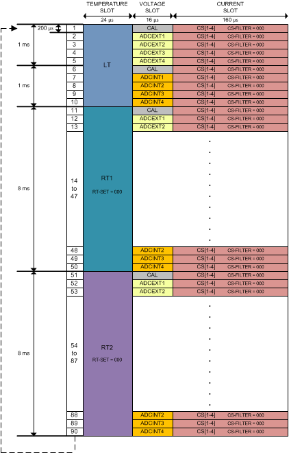 Figure 48. ADC General Interleaved Sequence
Each ADC interleave step takes 200 µs and is segmented intro three sensing slots: temperature, voltage and current. The temperature slot is 24 µs long and allocates the temperature sensing channel conversions (internal temperature sensor and two remote temperature sensors) following the order LT → RT1 → RT2 → LT → ... If one of the temperature channels is not selected for conversion it is skipped. For example, if RT1 is not selected for conversion, the temperature slot conversion sequence is LT → RT2 → LT → ... Figure 48 illustrates the conversion sequence for the lowest remote temperature sensor update time, which is configured by setting RT-SET[2:0] = 000 in register 0x10. If a longer temperature sensor is selected to improve measurement accuracy a higher number of interleave steps is allocated for the remote temperature sensors.
The voltage slot takes 16 µs and allocates the four external inputs and four DAC monitoring internal inputs conversions. The external inputs, if enabled, are converted first. If none of the channels in a group (external or internal) are selected, no time is allocated for conversion of that group. However if at least one of the input channels in a group is enabled, five interleave steps (1 ms) are allocated regardless of the total number of input channels.
The current slot allocates the four current sensing channel conversions. The current slot is 160 µs long independent of how many current sense channels are enabled. The current sensors are updated on each interleave step (200 µs) when the CS-FILTER[2:0] set to 000 in register 0x10. If a longer current sense update time is selected to improve measurement accuracy a higher number of interleave steps is allocated for the current sense conversions.
The update time for all monitoring inputs is determined by the interleave sequence followed. Direct-mode conversions require an additional 40 µs of update time. In order to simplify synchronization, the AMC7834 provides a data-available signal through the DAV/ADC_RDY pin. The DAV/ADC_RDY pin must first be enabled through the DAVPIN-EN bit in register 0x11. Furthermore the DAV functionality must be selected by clearing the DAVPIN-SEL bit in register 0x11 to '0'.
In direct-mode conversion the DAV/ADC_RDY pin goes low after the conversion sequence has been completed. Additionally, in direct-mode conversion the data available flags in the General status register (address 0x1F) can be used to determine when new data is available for each data-available channel group. In autonomous conversion the DAV/ADC_RDY pin indicates when new data is available for each data-available channel group by issuing a 20 µs pulse (active low).
In both conversion methods the data-available function identifies six channel groups:
- Current sense inputs: CS1 through CS4
- External analog inputs: ADC1 through ADC4
- Internal monitoring inputs: ADCINT1 through ADCINT4
- Internal temperature sensor: LT
- Remote temperature sensor 1: RT1
- Remote temperature sensor 2: RT2
7.3.3 Temperature Sensors
The AMC7834 device includes one on-chip and two remote temperature sensors. The temperature sensors monitor the three temperature inputs. The on-chip integrated temperature sensor measures the device temperature and two remote diode-sensor inputs measure two external temperature points. All three temperature-sensor results are converted by the device ADC and stored in two’s complement format. If any sensor is not used, it can be disabled in the register configuration. When any of the temperature sensors is disabled it is not converted by the ADC.
7.3.3.1 Internal Temperature Sensor
The AMC7834 device has an on-chip temperature sensor that measures the device die temperature. The temperature-sensor results are converted by the device ADC (see the Analog-to-Digital Converter (ADC) section for more information). If internal temperature sensor conversion is not needed, it can be disabled in the ADC MUX register (address 0x12). When disabled the temperature sensor output is not converted by the ADC.
The temperature sensor provides 0.25°C resolution over the device operating temperature range. Additionally, the AMC7834 internal temperature sensor is specified monotonic down to –55°C. The temperature value is stored in 12-bit two’s complement format in the LT-data register (address 0x2D).
Table 3. Temperature Sensor Data Format
| TEMPERATURE (°C) | DIGITAL CODE |
|---|---|
| –55 | 1111 0010 0100 |
| –40 | 1111 0110 0000 |
| –25 | 1111 1001 1100 |
| –10 | 1111 1101 1000 |
| –0.25 | 1111 1111 1111 |
| 0 | 0000 0000 0000 |
| 0.25 | 0000 0000 0001 |
| 10 | 0000 0010 1000 |
| 25 | 0000 0110 0100 |
| 50 | 0000 1100 1000 |
| 75 | 0001 0010 1100 |
| 100 | 0001 1001 0000 |
| 105 | 0001 1010 0100 |
| 125 | 0001 1111 0100 |
Use Equation 4 and Equation 5 to calculate the positive or negative temperature according to the polarity of the temperature data MSB (0 = positive, 1 = negative).


7.3.3.2 Remote Temperature Sensors
The AMC7834 device includes two remote junction-temperature sensors. The remote sensing transistors can be a discrete, small-signal type transistor or a substrate transistor built within the power amplifier. These transistors are typically low-cost NPN- or PNP-type transistors such as the 2N3904 and 2N3906. Figure 49 shows the recommended connection for NPN and PNP transistors in diode configuration.
The AMC7834 device also allows PNP transistor configuration as shown in Figure 50. PNP transistor configuration for both remote temperature sensors is enabled by setting the RMT-GND-COLL bit to 1 in register 0x11.
NOTE
Pins D1– and D2– are internally shorted. Total parasitic capacitance to AGND on these pins must be less than 800 pF.
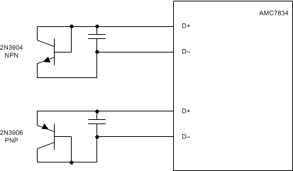 Figure 49. NPN and PNP Diode Configuration
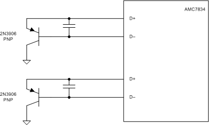 Figure 50. PNP Transistor Configuration
Errors in remote temperature sensor readings are typically the consequence of misalignment in the ideality factor and current excitation used by the AMC7834 versus the manufacturer-specified operating current for a given transistor. Some manufacturers specify a low-level (ILOW) and high-level (IHIGH) current for the temperature-sensing substrate transistors. The AMC7834 uses an ILOW of 7 µA and IHIGH of 112 µA and is designed to work with discrete transistors, such as the 2N3904 and SN3906. If an alternative transistor is used, the following conditions should be met:
- Base-emitter voltage (VBE) > 0.25 V at 7 µA for the highest sensed temperature
- Base-emitter voltage (VBE) < 1.20 V at 112 µA for the lowest sensed temperature
- Base resistance < 100 Ω
- Tight control of VBE characteristics indicated by small variations in hFE (50 to 150)
The ideality factor (η) is a measured characteristic of a remote temperature sensor diode as compared to an ideal one. The AMC7834 is trimmed for η = 1.008. If the selected remote sensing transistor's ideality factor is different, the effective η-factor should be adjusted at the system level.
Remote junction-temperature sensors are usually implemented in a noisy environment. Noise is most often created by fast digital signals and can corrupt measurements. A bypass capacitor placed differentially across the inputs of the remote temperature sensors can make the application more robust against unwanted coupled signals. If filtering is required, its time constant, including any routing resistance, should be limited to 5 µs or less. The combined series resistance on the remote temperature sensor pins must be less than 1 kΩ.
The two remote temperature sensor results are converted by the device ADC (see the Analog-to-Digital Converter (ADC) section for more information). The two remote temperature sensors can be disabled in the ADC MUX register (address 0x12). When disabled, the remote temperature sensor outputs are not converted by the ADC. The remote temperature values are stored in 12-bit two’s complement format in the RT-data registers (address 0x2E and 0x2F) using the same data format as the internal temperature sensor (see Table 3).
The AMC7834 device enables optimization of the remote temperature measurements by increasing the update time. The remote temperature-sensor update time is selected by the RT-SET[2:0] setting in register 0x10. Table 4 lists the total update time for the two remote temperature sensors with respect to the RT-SET[2:0] setting.
Table 4. Two Remote Temperature Sensors Update Time
| RT-SET[2:0] | TOTAL UPDATE TIME (ms) |
|---|---|
| 000 | 16 |
| 001 | 16 |
| 010 | 18 |
| 011 | 26 |
| 100 | 50 |
| 101 | 98 |
| All others | Not valid |
Optimal remote temperature sensor accuracy is achieved with the current-sense inputs disabled. In applications requiring simultaneous current-sensor and remote temperature sensor conversions it is recommended to implement external remote temperature conversion averaging to attain best accuracy results.
7.3.4 Current Sensors
The AMC7834 device integrates four unidirectional high-side current-sense amplifiers that amplify a small differential voltage developed across a current-sense resistor in the presence of high-input common-mode voltages. The AMC7834 current-sense amplifiers accept input signals with a common-mode voltage range from 4 V to 60 V. Each amplifier can operate with differential voltages up to 200 mV.
As shown in Figure 51, current flowing through RSENSE develops a voltage drop, VSENSE. The voltage across the sense resistor, VSENSE, is applied to one of the AMC7834 current-sense amplifier inputs. The current sense inputs should be connected as closely as possible to the shunt resistor to minimize any resistance in series with the shunt resistance.
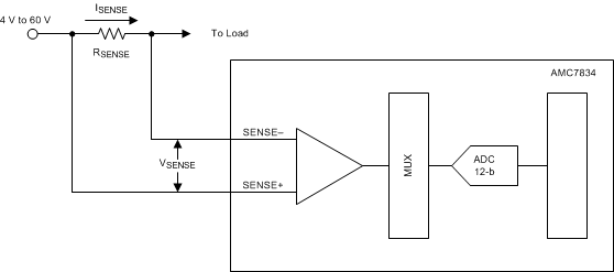 Figure 51. AMC7834 Current-Sense Amplifier
The accuracy of the current measurement depends heavily on the accuracy of the shunt resistor, R(SENSE). The use of a Kelvin sense resistor is highly recommended (see Figure 52).
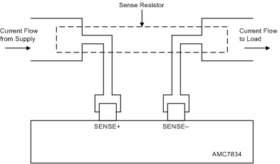 Figure 52. Kelvin Connection to the Sense Resistor
The sense-resistor value is application dependent and is typically a compromise between small-signal accuracy, maximum permissible voltage drop, and allowable power dissipation in the current measurement circuit. For best results, the value of the resistor is calculated from the maximum-expected load current, ILmax, and the maximum differential voltage supported by the current-sense amplifier (200 mV). High values of R(SENSE) provide better accuracy at lower currents by minimizing the effects of the current-sense amplifier offset. Low values of R(SENSE) minimize load voltage loss, but at the expense of low current accuracy. In general, a compromise between low current accuracy and load circuit losses must be made.
The maximum differential voltage, VSENSE, supported by the AMC7834 current-sense amplifiers is 200 mV. Use Equation 6 to calculate the R(SENSE) value.
The maximum power dissipation of the sense resistor should not be exceeded. Use Equation 7 to calculate the maximum sense resistor power dissipation.
The current sensors operate as four standalone current-sense amplifiers when the AMC7834 is set in open-loop mode (LOOP-EN bit set to 0 in register 0x10). In open-loop mode the current-sense amplifier outputs are converted by the device ADC and the results are stored in straight binary format in the CS-Data registers (address 0x29 through 0x2B). Use Equation 8 to calculate the differential voltage, VSENSE.

Alternatively, with the AMC7834 set in closed-loop mode (LOOP-EN bit set to 1 in register 0x10) the current sensors operate as part of four independent closed-loop current controllers. In closed-loop operation, four autonomous closed-loop current controllers are implemented by continuously adjusting the bipolar DAC outputs in response to the current-sense amplifier outputs (see the Closed-Loop Mode section).
The AMC7834 device enables digital filtering of the current sense measurements to improve their accuracy at the cost of a longer update time. The current sense digital filter is enabled by the CS-FILTER[2:0] setting in register 0x10 and its corresponding transfer function is given by Equation 9.

Table 5 lists the K value associated with each of the allowable CS-FILTER[2:0] settings as well as the corresponding update time.
Table 5. Current Sense Digital Filter Configuration
| CS-FILTER[2:0] | K | UPDATE TIME (ms) |
|---|---|---|
| 000 | 1 | 0.2 |
| 001 | 2 | 3.4 |
| 010 | 4 | 6.6 |
| 011 | 8 | 13 |
| 100 | 16 | 25.6 |
| All others | Not valid | |
7.3.5 Drain Switch Control
The AMC7834 device includes an output-control voltage (PA_ON pin) capable of driving an external PMOS switch that turns on and off the drain current to a PA FET. The use of this control signal in conjunction with the DAC clamp option allows control of the sequence in which the PA FET is powered up and powered down.
The OFF and ON states of the PA_ON signal are equal to the PAVDD and AGND pins, respectively. The default state of the PA_ON signal is off (PMOS switch off).
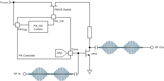 Figure 53. PA_ON Operation
The maximum output voltage is determined by the PAVDD pin and limited to a maximum of 20 V. For PA FETs with drain voltages higher than 20 V, tying the PAVDD pin to one of the other supply devices (preferably AVDD) and scaling the control signal externally is recommended.
The PA_ON signal state can be set through a register write, but it can also be configured to be triggered automatically by the ALARMOUT pin, any of the SLEEP signals or by the special AVSS and AVDD monitoring circuits.
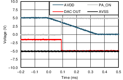
For FETs requiring a negative bias voltage, such as GaN, ensuring that the bias voltage remains within an acceptable range is crucial otherwise significant and irreversible damage to the FET can occur. The AMC7834 bipolar DAC operation and clamping mechanism rely on the AVDD and AVSS voltages for proper operation. For this reason, when either the AVDD or AVSS voltage falls outside its acceptable range, turning off the drain current to the FET is desirable.
The AVDD detection circuit is set to trigger the PA_ON signal to the OFF state in response to an out of range event. Additionally, the AVSS detection alarm can be set to trigger the PA_ON signal to the OFF state by setting the PAON_AVSS bit to 1 in the AMC configuration 1 register (address 0x11). The AVSS alarm is set by default to prevent the PA_ON output from entering the ON state (PMOS switch on). In this case writing to the PA_ON register bit to enable the ON state is ignored. If this additional protection is not needed it can be disabled by clearing the PAON_AVSS bit.
7.3.6 Programmable Out-of-Range Alarms
The AMC7834 device is capable of continuously analyzing the four internal ADC monitoring inputs (bipolar DAC-output monitoring), current sensors, temperature sensors, and negative supply for normal operation.
Normal operation is established through the lower and upper threshold registers (address 0x40 through 0x4D). When any of the monitored inputs is out of the specified range, an alarm event is issued and the global alarm bit, GALARM in the General Status register (address 0x1F), is set (see Figure 54). The alarm status register (address 0x1E) indicates the source of the alarm event.
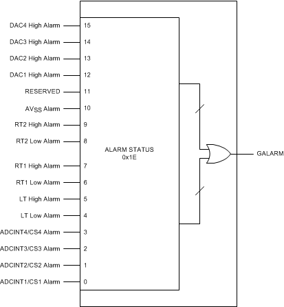 Figure 54. AMC7834 Alarm Status Register
The ALARM-LATCH-DIS bit in the ALARMOUT configuration register (address 0x1B) sets the latching behavior for all alarms. When the ALARM-LATCH-DIS bit is cleared to 0 the alarm bits in the alarm status register are latched. The alarm bits are referred to as being latched because the bits remain set until read by software. This design ensures that out-of-limit events cannot be missed if the software is periodically polling the device. All bits are cleared when reading the alarm status register, and all bits are reasserted if the out-of limit condition still exists on the next monitoring cycle, unless otherwise noted. When the ALARM-LATCH-DIS bit is set to 1, the alarm bits are not latched. The alarm bits in the alarm status register are set to 0 when the error condition subsides, regardless of whether the bit is read or not.
All of the alarms can be set to activate the ALARMOUT pin. The ALARMOUT pin is an open-drain pin and therefore an external pullup resistor to a voltage no higher than that of the AVDD pin is required. The ALARMOUT output polarity is defined through the ALARMOUT-POLARITY bit in the ALARMOUT configuration register (address 0x1B). The default polarity is active low (ALARMOUT-POLARITY = 0). The polarity can be changed to active high by setting the ALARMOUT-POLARITY bit to 1. The ALARMOUT pin works as an interrupt to the host so that it can query the alarm status register to determine the alarm source. Any alarm event can activate the pin as long as the alarm is not masked in the ALARMOUT configuration register. When an alarm event is masked, the occurrence of the event sets the corresponding status bit in the alarm status register, but does not activate the ALARMOUT pin.
The ALARMOUT status can be configured to automatically clamp specific DACs or set the PA_ON signal to the OFF state. The ALARMOUT clamp register selects the DAC or DAC pairs that enter the clamp mode as well as the PA_ON behavior when the ALARMOUT pin is active. Clearing the alarm events does not automatically bring the DAC or DAC pairs back to normal operation or return the PA_ON to the ON state.
7.3.6.1 ADC Internal Monitoring Input Out-of-Range Alarm
The AMC7834 device can provide out-of-range detection for the four internal ADC inputs monitoring the bipolar DAC outputs when operating in closed-loop mode. The ADCINT/CS-SELECT bit in register 0x1B must be cleared to 0 to enable out-of-range detection on the internal ADC inputs.
Figure 55 shows the out-of-range detection block. When the measurement is out-of-range, the corresponding alarm bit in the alarm status register is set to 1 to flag the out-of-range condition. The values in the ADCINTn/CSn upper and lower threshold registers (address 0x40 through 0x47) define the upper- and lower-bound thresholds for these inputs when the ADCINT/CS-SELECT bit in the ALARMOUT configuration register (address 0x1B) is cleared to 0.
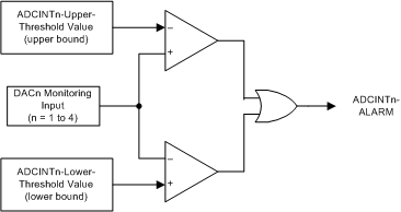 Figure 55. ADC Monitoring Out-of-Range Alarm
7.3.6.2 Current-Sense Out-of-Range Alarm
The AMC7834 device is capable of providing out-of-range detection for the four current-sense inputs when operating in open-loop mode. The current-sense out-of-range detection is only active if the ADCINT/CS-SELECT bit in register 0x1B is set to 1.
Figure 56 shows the current sense detection block. When the measurement is out-of-range, the corresponding alarm bit in the alarm status register is set to 1 to flag the out-of-range condition. The values in the ADCINTx/CSx upper and lower threshold registers (address 0x40 through 0x47) define the upper- and lower-bound thresholds for these inputs when the ADCINT/CS-SELECT bit in the ALARMOUT configuration register (address 0x1B) is set to 1.
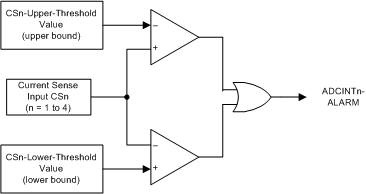 Figure 56. Current-Sense Out-of-Range Alarm
7.3.6.3 Temperature Sensors Out-of-Range Alarm
The AMC7834 device also includes high-limit or low-limit detection for the temperature sensors. Figure 57 shows the temperature detection block. The values in the temperature sensors upper and lower threshold registers (address 0x48 through 0x4D) set the limits for the temperature sensors. The temperature sensors can issue either a high alarm (HIGH-ALARM bit) or a low alarm (LOW-ALARM bit) in the alarm status register (address 0x1E) depending on whether the high or low thresholds were exceeded. To implement single, upper-bound threshold detection for the temperature sensors, the host processor can set the upper-bound threshold to the desired value and the lower-bound threshold to the default value. For lower-bound threshold detection, the host processor can set the lower-bound threshold to the desired value and the upper-bound threshold to the default value.
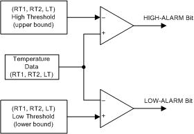 Figure 57. Temperature Out-of-Range Alarm
7.3.6.4 Bipolar DACs High Alarm
The AMC7834 device includes configurable upper-limit detection for the bipolar DACs in closed-loop mode. Figure 58 shows the alarm detection block. The values in the bipolar DAC upper threshold registers (address 0x4E through 0x4F) set a limit other than full-scale limit for the bipolar DACs. When a closed-loop controller attempts to set its bipolar DAC to a value exceeding the corresponding upper-threshold register, the DAC is instead updated with the threshold value and a DAC high-alarm is issued in the alarm status register.
 Figure 58. Bipolar DAC High Alarm
7.3.6.5 AVSS Detection Alarm
The device continuously monitors the AVSS supply to ensure it is within the required operating threshold. By setting the PAON_AVSS bit to 1 in the AMC configuration 1 register (address 0x11) the AVSS alarm can be set to automatically set the PA_ON pin to the OFF state and prevent it from getting configured back to the ON state unless the AVSS alarm has been cleared.
7.3.6.6 AVDD Detection Alarm
The device continuously monitors the AVDD supply to ensure it is within the required operating threshold. An AVDD alarm initiates a POR event which sets the PA_ON pin to the OFF state, bipolar DACs to the AVSS clamp mode and auxiliary DACs to clamp mode.
7.3.6.7 Hysteresis
If a monitored signal is out of range and the alarm is enabled, the corresponding alarm bit is set to 1. However, the alarm condition is cleared only when the conversion result returns either a value lower than the high threshold register setting or higher than the low threshold register setting by the number of codes specified in the hysteresis setting (Figure 59). The hysteresis registers (address 0x50 through 0x56) store the hysteresis value for the programmable alarms. The hysteresis is a programmable value between 0 LSB to 127 LSB for the internal ADC monitoring and current-sense alarms and 0°C to 31°C for the temperature-sensor alarms.
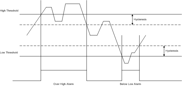 Figure 59. Device Hysteresis
7.3.6.8 False-Alarm Protection
To prevent false alarms, an alarm event is only registered when the monitored signal is out of range for an N number of consecutive conversions. If the monitored signal returns to the normal range before N consecutive conversions, an alarm event is not issued. The false alarm factor, N, can be configured in the AMC configuration 1 register (address 0x11).
7.3.7 Reference Specifications
The AMC7834 device includes a high-performance 2.5 V reference. Operation from an external reference is also supported.
7.3.7.1 Internal Reference Operation
The AMC7834 device includes a 2.5 V bipolar transistor-based, precision bandgap reference. The internal reference is externally available at the REF_OUT pin and can be used to drive the ADC and eight DACs by connecting the REF_OUT pin to the REF_IN pin (see Figure 60). A 10-nF capacitor is recommended between REF_OUT and AGND for noise filtering. An external buffer amplifier with a high-impedance input must be used to drive any external load. A compensation capacitor (4.7 μF, typical) should be connected between the REF_CMP pin and the AGND4 pin.
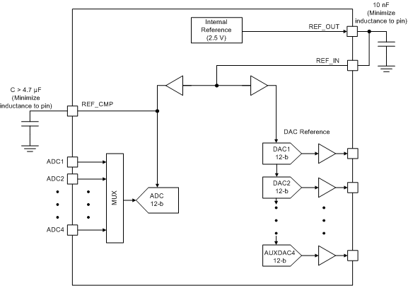 Figure 60. Internal Reference Operation
7.3.7.2 External Reference Operation
The AMC7834 device can also operate from an external reference. The external reference can be applied to the REF_IN pin and is used to drive both the ADC and the eight DACs through separate buffers (see Figure 61). As with the internal-reference case a compensation capacitor (4.7 μF, typical) should be connected between the REF_CMP pin and the AGND4 pin. The REF_OUT pin can be left floating if unused.
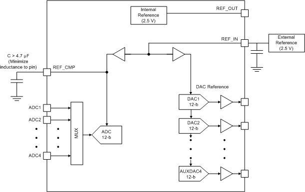 Figure 61. External Reference Operation
7.3.8 General Purpose I/Os
The AMC7834 device includes four GPIO pins. The GPIO pins can receive an input or produce an output (see Figure Figure 62). When the GPIOn pin acts as an output, it has an open-drain, and the status of this pin is determined by the corresponding GPIO bit in the GPIO register (address 0x58). The output state is high impedance when the GPIOn bit is set to 1, and is logic low when the GPIOn bit is cleared to 0.
NOTE
A 10-kΩ pullup resistor is required when using a GPIO pin as an output. The pullup voltage must not exceed the AVDD supply.
To use a GPIO pin as an input, the corresponding GPIO bit in the GPIO register must be set to 1. When a GPIO pin acts as input, the digital value on the pin is acquired by reading the corresponding GPIO bit. After a power-on reset or any forced reset, all GPIO bits are set to 1, and the GPIO pins enter a high impedance state.
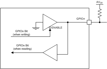 Figure 62. AMC7834 GPIO Pin
7.4 Device Functional Modes
The AMC7834 four high-side current-sense amplifiers and bipolar DACs operate in one of the following modes as selected by the LOOP-EN bit in register 0x10:
- Open-Loop Mode
- Closed-Loop Mode
7.4.1 Open-Loop Mode
The AMC7834 is set by default in open-loop mode. In open-loop mode, the current-sense amplifiers and bipolar DACs operate independently.
The AMC7834 four current sensors can operate with differential voltages up to 200 mV and accept common-mode voltages from 4 V to 60 V. The current-sense amplifier outputs are converted by the device ADC and the results are stored in straight binary format in the CS-Data registers (address 0x29 through 0x2B) to be accessed by a digital control device for further processing.
The AMC7834 four bipolar DACs are configured as DAC pairs (DAC1-DAC2 and DAC3-DAC4). The output range for each bipolar DAC pair can be configured through the DAC Range register to one of the following: 0 to 5 V, -5 to 0V, or -4 to 1 V. The POR and clamp value for each DAC pair is set by the pins VCLAMP1 (for the DAC1-DAC2 pair) and VCLAMP2 (for the DAC3-DAC4 pair) to any voltage between AVSS and 0 V. The full-scale output range of the bipolar DACs is limited by the power supplies, AVDD and AVSS. In open-loop mode the DAC output voltage is set by by a digital controller by writing the corresponding code in straight binary format to the DAC data registers (address 0x30 through 0x33).
Table 6 lists the typical register configurations for open-loop mode.
Table 6. Open-Loop Mode Register Configuration
| REGISTER SETTING | REGISTER ADDRESS | COMMENT |
|---|---|---|
| LOOP-EN | 0x10 | Set to 0 |
| CS-FILTER[2:0] | 0x10 | Configurable |
| ADCINTn | 0x12 | Set to 0 |
| LOOPn-SET[3:0] | 0x14 | Unused |
| DACn-SYNC | 0x15 | Configurable |
| ADCINT/CS-SELECT | 0x1B | Set to 1 |
| DACnnLOOP-ALARMEN | 0x1B | Set to 0 |
| DACn-HIGH-ALARM | 0x1E | Unused |
| ADCINTn-DATA[11:0] | 0x20 to 0x23 | Unused |
| CSn-DATA[11:0] | 0x28 to 0x2B | Readable |
| DACn-DATA[11:0] | 0x30 to 0x33 | Configurable |
| CLOSEDLOOPn[11:0] | 0x38 to 0x3B | Unused |
| DACnn-UP-THRES[11:0] | 0x4E to 0x4F | Unused |
7.4.2 Closed-Loop Mode
In closed-loop mode the current sensors and bipolar DACs operate as four independent closed-loop current controllers. In closed-loop operation, four autonomous closed-loop current controllers are implemented by continuously adjusting the bipolar DAC outputs in response to the current-sense amplifier outputs.
Table 7 lists the typical register configurations for closed-loop mode.
Table 7. Closed-Loop Mode Register Configuration
| REGISTER SETTING | REGISTER ADDRESS | COMMENT |
|---|---|---|
| LOOP-EN | 0x10 | Set to 1 |
| CS-FILTER[2:0] | 0x10 | Configurable |
| ADCINTn | 0x12 | Set to 1 |
| LOOPn-SET[3:0] | 0x14 | Configurable |
| DACn-SYNC | 0x15 | Unused |
| ADCINT/CS-SELECT | 0x1B | Set to 0 |
| DACnnLOOP-ALARMEN | 0x1B | Configurable |
| DACn-HIGH-ALARM | 0x1E | Used |
| ADCINTn-DATA[11:0] | 0x20 to 0x23 | Readable |
| CSn-DATA[11:0] | 0x28 to 0x2B | Unused |
| DACn-DATA[11:0] | 0x30 to 0x33 | Unused |
| CLOSEDLOOPn[11:0] | 0x38 to 0x3B | Configurable |
| DACnn-UP-THRES[11:0] | 0x4E to 0x4F | Configurable |
Figure 63 shows a typical analog implementation of a closed-loop current controller.
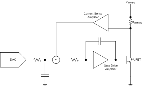 Figure 63. Analog Closed-Loop Current Controller
Although the analog current controller is capable of setting and maintaining a given drain current (and therefore, gain) through a PA FET it lacks the flexibility to scale easily to a large variety of FETs. The AMC7834 implements four closed-loop current controllers as a digital system thus giving it higher flexibility while satisfying or improving on the specifications given by a typical analog closed-loop current controller.
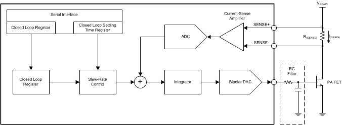 Figure 64. AMC7834 Closed-Loop Current Controller
Each of the four digital control loops consists of a digital integrator and a bipolar DAC in the forward path to drive the gate of a PA FET. A high-side current-sense amplifier in the feedback path senses the drain bias current and its output is converted by the device ADC.
As with the DACs in open-loop operation, the closed-loop current controllers can be set to clamp mode. When a current-controller goes into clamp mode the bipolar DAC output is immediately set to its corresponding clamp voltage and current-sense conversions are stopped. Note that with the exception of the current-sense inputs all other monitoring inputs continue to be converted by the device ADC while in clamp mode. Clamping does not clear the closed-loop state making it possible to return to the same voltage being output before the clamp event was issued.
Since the drain current does not immediately update in response to the out-of-clamp gate voltage, it is recommended to stop the ADC conversion prior to leaving the clamp state and re-starting conversion only after the drain current has stabilized. The stabilization time is dependent on the filtering at the bipolar DAC output and the PA FET characteristics.
The target drain current is set by the Closed Loop registers (address 0x38 to 0x3B) and is given by Equation 10.

where
- I(DRAIN) is the PA drain current (in Amperes)
- CLOSEDLOOPn[11:0] is the 12-bit digital code that is input to the control loop to set I(DRAIN)
- Vref is the device reference voltage
- R(SENSE) is the sense resistor resistance (in Ohms)
The control loop sets the target drain current by continuously maintaining a constant voltage across the shunt resistor (V(SENSE) = I(DRAIN) × R(SENSE)). The control loop continuously attempts to zero-out the error at the input of the integrator by adjusting the DAC output voltage and consequently keeping the drain current constant. Assuming negligible drift in the sense resistor, any variation in the drain current due to changes in the PA FET characteristics over time and temperature are automatically tracked and corrected.
Based on the target drain current and required PA gain ramp rate, the Closed Loop input code step can be divided by the slew-rate control block into smaller steps that are applied to the control loop every 200 μs. The slew-rate for each control loop is set by the Closed Loop Settling Time register (address 0x14). Issuing multiple, smaller code steps over time instead of one large code step helps achieve a more linear PA-gain ramp rate. Table 8 shows the control-loop settling time as a function of the slew-rate control setting.
Table 8. Closed-Loop Settling Time
| LOOPn-SET[3:0] | SETTLING TIME (ms) |
|---|---|
| 0000 | 0.8 |
| 0001 | 1.6 |
| 0010 | 2.4 |
| 0011 | 3.2 |
| 0100 | 4.8 |
| 0101 | 6.4 |
| 0110 | 9.6 |
| 0111 | 12.8 |
| 1000 | 19.2 |
| 1001 | 25.6 |
| 1010 | 28.8 |
| All others | Not valid |
Under normal conditions the code output by the slew-rate control block equals the ADC output in steady state. When the loop is disturbed as a result of a change on the target drain current or PA characteristics, the error between the slew-rate controller and ADC outputs is accumulated every 200 μs by the digital integrator. An optional external RC filter at the DAC output helps to smooth out the DAC steps at the input of the PA FET gate. The external filter time constant must be less than 50 µs.
The gain from the DAC output to the ADC input is given by Equation 11.
where
- gm(PA_FET) is the transconductance for the PA FET
This value should be less than 0.8 to ensure stability of the control loop.
7.5 Programming
The AMC7834 device is controlled through a flexible four-wire serial interface that is compatible with SPI-type interfaces used on many microcontrollers and DSP controllers. The interface provides read and write (R/W) access to all registers of the AMC7834 device.
Each serial-interface access cycle is exactly 24 bits long. A frame is initiated by asserting the CS pin low. The frame ends when the CS pin is deasserted high. The first bit transferred is the R/W bit. The next 7 bits are the register address (128 addressable registers), and the remaining 16 bits are data. For all writes, data is clocked in on the rising edge of SCLK. If the write access is not equal to 24 clocks, the data bits are not committed. On a read access, data is clocked out on the falling edge of the serial interface clock, SCLK, on the SDO pin.
Figure 65 and Figure 66 show the access protocol used by the interface. Data is accepted as MSB first.
 Figure 65. Serial Interface Write Bus Cycle
 Figure 66. Serial Interface Read Bus Cycle
7.6 Register Maps
Table 9. Memory Map
7.6.1 Power Mode: Address 0x02
7.6.1.1 Power Mode Register (address = 0x02) [reset = 0x000]
| 15 | 14 | 13 | 12 | 11 | 10 | 9 | 8 |
| Reserved | |||||||
| R/W-00h | |||||||
| 7 | 6 | 5 | 4 | 3 | 2 | 1 | 0 |
| Reserved | POWER-MODE | ||||||
| R/W-00h | R/W-00 | ||||||
Table 10. Power Mode Register Field Descriptions
| Bit | Field | Type | Reset | Description |
|---|---|---|---|---|
| 15-2 | Reserved | R/W | All zeros | Reserved for factory use. |
| 1–0 | POWER-MODE | R/W | 00 |
Power down mode for the AMC7834 device. See Table 11. |
Table 11. POWER-MODE Configuration
| POWER MODE | Value | Reference | Current Sensors | ADC | ADC Reference Buffer | DAC Reference Buffer | Auxiliary DACs | Bipolar DACs |
|---|---|---|---|---|---|---|---|---|
| Power-Down Mode | 0x | ON | OFF | OFF | OFF | OFF | OFF | ON |
| Active Mode | 10 | ON | ON | ON | ON | ON | ON | ON |
| Reserved Mode | 11 | Not valid. Reserved for factory use. | ||||||
7.6.2 Device Identification: Address 0x04 through 0x0C
7.6.2.1 Device ID Register (address = 0x04) [reset = 0x0C34]
| 15 | 14 | 13 | 12 | 11 | 10 | 9 | 8 |
| DEVICEID | |||||||
| R-0Ch | |||||||
| 7 | 6 | 5 | 4 | 3 | 2 | 1 | 0 |
| DEVICEID | |||||||
| R-34h | |||||||
Table 12. Device ID Register Field Descriptions
| Bit | Field | Type | Reset | Description |
|---|---|---|---|---|
| 15-0 | DEVICEID | R | 0C34h | Device ID. |
7.6.2.2 Version ID Register (address = 0x06) [reset = 0x0001]
7.6.2.3 Vendor ID Register (address = 0x0C) [reset = 0x0451]
| 15 | 14 | 13 | 12 | 11 | 10 | 9 | 8 |
| VENDORID | |||||||
| R-04h | |||||||
| 7 | 6 | 5 | 4 | 3 | 2 | 1 | 0 |
| VENDORID | |||||||
| R-51h | |||||||
Table 14. Vendor ID Register Field Descriptions
| Bit | Field | Type | Reset | Description |
|---|---|---|---|---|
| 15-0 | VENDORID | R | 0451h | Vendor ID. |
7.6.3 General Device Configuration: Address 0x10 through 0x16
7.6.3.1 AMC Configuration 0 Register (address = 0x10) [reset = 0x0300]
| 15 | 14 | 13 | 12 | 11 | 10 | 9 | 8 |
| Reserved | CMODE | Reserved | CS-FILTER[2:0] | ||||
| R/W-000 | R/W-0 | R/W-0 | R/W-011 | ||||
| 7 | 6 | 5 | 4 | 3 | 2 | 1 | 0 |
| Reserved | RT-SET[2:0] | Reserved | LOOP-EN | ||||
| R/W-0 | R/W-000 | R/W-000 | R/W-0 | ||||
Table 15. AMC Configuration 0 Field Descriptions
| Bit | Field | Type | Reset | Description |
|---|---|---|---|---|
| 15-13 | Reserved | R/W | 000 |
Reserved for factory use. |
| 12 | CMODE | R/W | 0 | 0: Autonomous ADC conversion 1: Direct-mode ADC conversion |
| 11 | Reserved | R/W | 0 |
Reserved for factory use. |
| 10-8 | CS-FILTER[2:0] | R/W | 011 |
Current sense filter setting. Improves noise of current sensors measurements by trading off the update time. The digital filter has the transfer function: Equation 12.
 See Table 16 for its configuration. |
| 7 | Reserved | R/W | 0 |
Reserved for factory use. |
| 6-4 | RT-SET[2:0] | R/W | 000 |
Improves noise of the remote temperature sensors measurements by trading off the update time. See Table 17 for its configuration. |
| 3-1 | Reserved | R/W | 000 |
Reserved for factory use. |
| 0 | LOOP-EN | R/W | 0 |
When set to 1 enables closed-loop mode operation. |
Table 16. CS-FILTER Configuration
| CS-FILTER[2:0] | K | Approximate Update Time (ms) |
|---|---|---|
| 000 | 1 | 0.2 |
| 001 | 2 | 3.4 |
| 010 | 4 | 6.6 |
| 011 | 8 (default) | 13 |
| 100 | 16 | 25.6 |
| All others | Not valid | |
Table 17. RT-SET Configuration
| RT-SET[2:0] | Two Remote Sensors Update Time (ms) |
|---|---|
| 000 | 16 |
| 001 | 16 |
| 010 | 18 |
| 011 | 26 |
| 100 | 50 |
| 101 | 98 |
| All others | Not valid |
7.6.3.2 AMC Configuration 1 Register (address = 0x11) [reset = 0x036A]
| 15 | 14 | 13 | 12 | 11 | 10 | 9 | 8 |
| DAVPIN-EN | DAVPIN-SEL | Reserved | CH-FALR[2:0] | ||||
| R/W-0 | R/W-0 | R/W-000 | R/W-011 | ||||
| 7 | 6 | 5 | 4 | 3 | 2 | 1 | 0 |
| RMT-GND-COLL | PAON_AVSS | LT-FALR[1:0] | RT2-FALR[1:0] | RT1-FALR[1:0] | |||
| R/W-0 | R/W-1 | R/W-10 | R/W-10 | R/W-10 | |||
Table 18. AMC Config1 Field Descriptions
| Bit | Field | Type | Reset | Description |
|---|---|---|---|---|
| 15 | DAVPIN-EN | R/W | 0 |
When set to 1 it enables the DAV/ADC_RDY pin output function. When cleared to 0 the DAV/ADC_RDY pin is in high impedance mode. |
| 14 | DAVPIN-SEL | R/W | 0 |
When cleared to 0 and if DAVPIN-EN is equal to 1 the DAV/ADC_RDY pin operates as a DAV pin. When set to 1 and if DAVPIN-EN is equal to 1 the DAV/ADC_RDY pin operates as an ADC_RDY pin. |
| 13-11 | Reserved | R/W | 000 |
Reserved for factory use. |
| 10 | CH-FALR[2:0] | R/W | 011 |
False alarm protection for ADC channels. Use the following configurations for the consecutive samples before the alarm is set: 001: 4 010: 8 011: 16 (default) 100: 32 101: 64 110: 128 111: 256 |
| 7 | RMT-GND-COLL | R/W | 0 |
When set to 1 enables PNP transistor configuration on both remote temperature sensors. |
| 6 | PAON_AVSS | R/W | 1 |
When PAON_AVSS = 1 an AVSS alarm event automatically switches the PA_ON pin to the OFF state. The AVSS alarm must be cleared before the PA_ON pin can be switch back to the ON state. When PAON_AVSS = 0 the PA_ON pin is unaffected by an AVSS alarm event. |
| 5-4 | LT-FALR[1:0] | R/W | 10 |
False alarm protection for local temperature sensor. Use the following configurations for the consecutive samples before the alarm is set: 01: 2 10: 4 (default) 11: 8 |
| 3-2 | RT2-FALR[1:0] | R/W | 10 |
False alarm protection for remote temperature sensor 2 (D2+, D2–). Use the following configurations for the consecutive samples before the alarm is set: 01: 2 10: 4 (default) 11: 8 |
| 1–0 | RT1-FALR[1:0] | R/W | 10 |
False alarm protection for remote temperature sensor 1 (D1+, D1–). Use the following configurations for the consecutive samples before the alarm is set: 01: 2 10: 4 (default) 11: 8 |
7.6.3.3 ADC MUX Register (address = 0x12) [reset = 0x0000]
| 15 | 14 | 13 | 12 | 11 | 10 | 9 | 8 |
| Reserved | LT | RT2 | RT1 | CS4 | CS3 | CS2 | CS1 |
| R/W-0 | R/W-0 | R/W-0 | R/W-0 | R/W-0 | R/W-0 | R/W-0 | R/W-0 |
| 7 | 6 | 5 | 4 | 3 | 2 | 1 | 0 |
| ADCEXT4 | ADCEXT3 | ADCEXT2 | ADCEXT1 | ADCINT4 | ADCINT3 | ADCINT2 | ADCINT1 |
| R/W-0 | R/W-0 | R/W-0 | R/W-0 | R/W-0 | R/W-0 | R/W-0 | R/W-0 |
Table 19. ADC MUX Register Field Descriptions
| Bit | Field | Type | Reset | Description |
|---|---|---|---|---|
| 15 | Reserved | R/W | 0 |
When set to 1 the corresponding analog input channel to the ADC mux is accessed during an ADC conversion cycle. When cleared to 0 the corresponding input channel to the ADC mux is ignored during an ADC conversion cycle. |
| 14 | LT | R/W | 0 | |
| 13 | RT2 | R/W | 0 | |
| 12 | RT1 | R/W | 0 | |
| 11 | CS4 | R/W | 0 | |
| 10 | CS3 | R/W | 0 | |
| 9 | CS2 | R/W | 0 | |
| 8 | CS1 | R/W | 0 | |
| 7 | ADCEXT4 | R/W | 0 | |
| 6 | ADCEXT3 | R/W | 0 | |
| 5 | ADCEXT2 | R/W | 0 | |
| 4 | ADCEXT1 | R/W | 0 | |
| 3 | ADCINT4 | R/W | 0 | |
| 2 | ADCINT3 | R/W | 0 | |
| 1 | ADCINT2 | R/W | 0 | |
| 0 | ADCINT1 | R/W | 0 |
7.6.3.4 Closed Loop Settling Time Register (address = 0x14) [reset = 0x2222]
| 15 | 14 | 13 | 12 | 11 | 10 | 9 | 8 |
| LOOP4-SET[3:0] | LOOP3-SET[3:0] | ||||||
| R/W-0010 | R/W-0010 | ||||||
| 7 | 6 | 5 | 4 | 3 | 2 | 1 | 0 |
| LOOP2-SET[3:0] | LOOP1-SET[3:0] | ||||||
| R/W-0010 | R/W-0010 | ||||||
Table 20. Closed Loop Settling Time Register Field Descriptions
| Bit | Field | Type | Reset | Description |
|---|---|---|---|---|
| 15-12 | LOOP4-SET[3:0] | R/W | 0010 |
Slew rate controller. Sets the maximum voltage transition rate of each closed-loop current controller. See Table 21 for its configuration. |
| 11–8 | LOOP3-SET[3:0] | R/W | 0010 | |
| 7-4 | LOOP2-SET[3:0] | R/W | 0010 | |
| 3-0 | LOOP1-SET[3:0] | R/W | 0010 |
Table 21. Closed-Loop Settling Time Configuration
| LOOPn-SET[3:0] | Settling Time (ms) |
|---|---|
| 0000 | 0.8 |
| 0001 | 1.6 |
| 0010 | 2.4 |
| 0011 | 3.2 |
| 0100 | 4.8 |
| 0101 | 6.4 |
| 0110 | 9.6 |
| 0111 | 12.8 |
| 1000 | 19.2 |
| 1001 | 25.6 |
| 1010 | 28.8 |
| All others | Not valid |
7.6.3.5 DAC Sync Register (address = 0x15) [reset = 0x0000]
| 15 | 14 | 13 | 12 | 11 | 10 | 9 | 8 |
| Reserved | |||||||
| R/W-00h | |||||||
| 7 | 6 | 5 | 4 | 3 | 2 | 1 | 0 |
| AUXDAC4-SYNC | AUXDAC3-SYNC | AUXDAC2-SYNC | AUXDAC1-SYNC | DAC4-SYNC | DAC3-SYNC | DAC2-SYNC | DAC1-SYNC |
| R/W-0 | R/W-0 | R/W-0 | R/W-0 | R/W-0 | R/W-0 | R/W-0 | R/W-0 |
Table 22. DAC Sync Register Field Descriptions
| Bit | Field | Type | Reset | Description |
|---|---|---|---|---|
| 15-8 | Reserved | R/W | 0x00 |
Reserved for factory use. |
| 7 | AUXDAC4-SYNC | R/W | 0 |
When set to 1 the corresponding DAC output is set to synchronous-mode. When cleared to 0 the corresponding DAC output is set to asynchronous-mode. In closed-loop mode DAC1, DAC2, DAC3 and DAC4 are always in asynchronous-mode. |
| 6 | AUXDAC3-SYNC | R/W | 0 | |
| 5 | AUXDAC2-SYNC | R/W | 0 | |
| 4 | AUXDAC1-SYNC | R/W | 0 | |
| 3 | DAC4-SYNC | R/W | 0 | |
| 2 | DAC3-SYNC | R/W | 0 | |
| 1 | DAC2-SYNC | R/W | 0 | |
| 0 | DAC1-SYNC | R/W | 0 |
7.6.3.6 DAC Range Register (address = 0x16) [reset = 0x0000]
| 15 | 14 | 13 | 12 | 11 | 10 | 9 | 8 |
| Reserved | |||||||
| R/W-00h | |||||||
| 7 | 6 | 5 | 4 | 3 | 2 | 1 | 0 |
| AUXDAC4-RANGE | AUXDAC3-RANGE | AUXDAC2-RANGE | AUXDAC1-RANGE | DAC34-RANGE[1:0] | DAC12-RANGE[1:0] | ||
| R/W-0 | R/W-0 | R/W-0 | R/W-0 | R/W-00 | R/W-00 | ||
Table 23. DAC Range Register Field Descriptions
| Bit | Field | Type | Reset | Description |
|---|---|---|---|---|
| 15-8 | Reserved | R/W | 0x00 |
Reserved for factory use. |
| 7 | AUXDAC4-RANGE | R/W | 0 |
When cleared to 0 the corresponding AUXDAC output range is 0 to 5 V. When set to 1 the corresponding AUXDAC output range is 2.5 to 7.5 V. |
| 6 | AUXDAC3-RANGE | R/W | 0 | |
| 5 | AUXDAC2-RANGE | R/W | 0 | |
| 4 | AUXDAC1-RANGE | R/W | 0 | |
| 3-2 | DAC34-RANGE[1:0] | R/W | 00 | Sets the bipolar DAC output range. Use the following configurations for the DAC output range: 00: –4 to 1 V 01: –5 to 0 V 10: –5 to 0 V 11: 0 to 5 V |
| 1–0 | DAC12-RANGE[1:0] | R/W | 00 |
7.6.4 Clamp and Alarm Configuration: Address 0x17 through 0x1B
7.6.4.1 CLAMP Configuration Register (address = 0x17) [reset = 0x003F]
| 15 | 14 | 13 | 12 | 11 | 10 | 9 | 8 |
| Reserved | |||||||
| R/W-00h | |||||||
| 7 | 6 | 5 | 4 | 3 | 2 | 1 | 0 |
| Reserved | PAON | AUXDAC4-CLAMP | AUXDAC3-CLAMP | AUXDAC2-CLAMP | AUXDAC1-CLAMP | DAC34-CLAMP | DAC12-CLAMP |
| R/W-0 | R/W-0 | R/W-1 | R/W-1 | R/W-1 | R/W-1 | R/W-1 | R/W-1 |
Table 24. CLAMP Configuration Field Descriptions
| Bit | Field | Type | Reset | Description |
|---|---|---|---|---|
| 15-7 | Reserved | R/W | All zeros |
Reserved for factory use. |
| 6 | PAON | R/W | 0 |
Direct control of the PA_ON pin. When cleared to 0 the PA_ON pin is in the OFF state (PAVDD). When set to 1 the PA_ON pin is in the ON state (AGND). When read, the value of this bit reflects the state of the PA_ON pin. |
| 5 | AUXDAC4-CLAMP | R/W | 1 |
This register uses software to force the corresponding DAC into clamp. If 1, the corresponding DAC or DAC pair is forced into clamp. If 0, the corresponding DAC or DAC pair is restored to normal operation. If a DAC or DAC pair is in clamp mode through a SLEEP pin the corresponding clamp bit is automatically set to 1. |
| 4 | AUXDAC3-CLAMP | R/W | 1 | |
| 3 | AUXDAC2-CLAMP | R/W | 1 | |
| 2 | AUXDAC1-CLAMP | R/W | 1 | |
| 1 | DAC34-CLAMP | R/W | 1 | |
| 0 | DAC12-CLAMP | R/W | 1 |
7.6.4.2 SLEEP1 Configuration Register (address = 0x18) [reset = 0xFF00]
| 15 | 14 | 13 | 12 | 11 | 10 | 9 | 8 |
| Reserved | PAON-SNOOZE1 | AUXDAC4-SNOOZE1 | AUXDAC3-SNOOZE1 | AUXDAC2-SNOOZE1 | AUXDAC1-SNOOZE1 | DAC34-SNOOZE1 | DAC12-SNOOZE1 |
| R/W-1 | R/W-1 | R/W-1 | R/W-1 | R/W-1 | R/W-1 | R/W-1 | R/W-1 |
| 7 | 6 | 5 | 4 | 3 | 2 | 1 | 0 |
| Reserved | PAON-SLEEP1 | AUXDAC4-SLEEP1 | AUXDAC3-SLEEP1 | AUXDAC2-SLEEP1 | AUXDAC1-SLEEP1 | DAC34-SLEEP1 | DAC12-SLEEP1 |
| R/W-0 | R/W-0 | R/W-0 | R/W-0 | R/W-0 | R/W-0 | R/W-0 | R/W-0 |
Table 25. SLEEP1 Configuration Field Descriptions
| Bit | Field | Type | Reset | Description |
|---|---|---|---|---|
| 15 | Reserved | R/W | 1 |
Reserved for factory use. |
| 14 | PAON-SNOOZE1 | R/W | 1 |
Setting this bit to 1 imposes an additional write to the PA_ON register to set the PA_ON pin to the ON state after clearing the SLEEP1 pin. Setting this bit to 0 enables the SLEEP1 pin to set the PA_ON pin to the ON state directly. |
| 13 | AUXDAC4-SNOOZE1 | R/W | 1 |
Setting any of these bits to 1 imposes an additional write to the CLAMP Configuration register to wake-up the corresponding DAC or DAC pair from clamp after clearing the SLEEP1 pin. Clearing any of these bits to 0 enables the SLEEP1 pin to wake-up the DAC or DAC pairs directly. |
| 12 | AUXDAC3-SNOOZE1 | R/W | 1 | |
| 11 | AUXDAC2-SNOOZE1 | R/W | 1 | |
| 10 | AUXDAC1-SNOOZE1 | R/W | 1 | |
| 9 | DAC34-SNOOZE1 | R/W | 1 | |
| 8 | DAC12-SNOOZE1 | R/W | 1 | |
| 7 | Reserved | R/W | 0 |
Reserved for factory use |
| 6 | PAON-SLEEP1 | R/W | 0 |
Setting this bit to 1 allows control of the PA_ON pin through the SLEEP1 pin. When SLEEP1 pin goes high the PA_ON pin enters the OFF state. Bringing the SLEEP1 pin low is required but not necessarily sufficient to return the PA_ON pin to the ON state as determined by the SNOOZE bits. Setting this bit to 0 causes the PA_ON pin to be unaffected by the SLEEP1 pin. |
| 5 | AUXDAC4-SLEEP1 | R/W | 0 |
Setting any of these bits to 1 allows control of the corresponding DAC or DAC pair through the SLEEP1 pin. When SLEEP1 pin goes high the DAC or DAC pair goes into clamp mode. Bringing the SLEEP1 pin low is required but not necessarily sufficient to return the DAC or DAC pairs to normal operation as determined by the SNOOZE bits. Clearing any of these bits to 0 causes the corresponding DAC or DAC pair to be unaffected by the SLEEP1 pin. |
| 4 | AUXDAC3-SLEEP1 | R/W | 0 | |
| 3 | AUXDAC2-SLEEP1 | R/W | 0 | |
| 2 | AUXDAC1-SLEEP1 | R/W | 0 | |
| 1 | DAC34-SLEEP1 | R/W | 0 | |
| 0 | DAC12-SLEEP1 | R/W | 0 |
7.6.4.3 SLEEP2 Configuration Register (address = 0x19) [reset = 0xFF00]
| 15 | 14 | 13 | 12 | 11 | 10 | 9 | 8 |
| Reserved | PAON-SNOOZE2 | AUXDAC4-SNOOZE2 | AUXDAC3-SNOOZE2 | AUXDAC2-SNOOZE2 | AUXDAC1-SNOOZE2 | DAC34-SNOOZE2 | DAC12-SNOOZE2 |
| R/W-1 | R/W-1 | R/W-1 | R/W-1 | R/W-1 | R/W-1 | R/W-1 | R/W-1 |
| 7 | 6 | 5 | 4 | 3 | 2 | 1 | 0 |
| Reserved | PAON-SLEEP2 | AUXDAC4-SLEEP2 | AUXDAC3-SLEEP2 | AUXDAC2-SLEEP2 | AUXDAC1-SLEEP2 | DAC34-SLEEP2 | DAC12-SLEEP2 |
| R/W-0 | R/W-0 | R/W-0 | R/W-0 | R/W-0 | R/W-0 | R/W-0 | R/W-0 |
Table 26. SLEEP2 Configuration Field Descriptions
| Bit | Field | Type | Reset | Description |
|---|---|---|---|---|
| 15 | Reserved | R/W | 1 |
Reserved for factory use |
| 14 | PAON-SNOOZE2 | R/W | 1 |
Setting this bit to 1 imposes an additional write to the PA_ON register to set the PA_ON pin to the ON state after clearing the SLEEP2 pin. Setting this bit to 0 enables the SLEEP2 pin to set the PA_ON pin to the ON state directly. |
| 13 | AUXDAC4-SNOOZE2 | R/W | 1 |
Setting any of these bits to 1 imposes an additional write to the CLAMP Configuration register to wake-up the corresponding DAC or DAC pair from clamp after clearing the SLEEP2 pin. Clearing any of these bits to 0 enables the SLEEP2 pin to wake-up the DAC or DAC pairs directly. |
| 12 | AUXDAC3-SNOOZE2 | R/W | 1 | |
| 11 | AUXDAC2-SNOOZE2 | R/W | 1 | |
| 10 | AUXDAC1-SNOOZE2 | R/W | 1 | |
| 9 | DAC34-SNOOZE2 | R/W | 1 | |
| 8 | DAC12-SNOOZE2 | R/W | 1 | |
| 7 | Reserved | R/W | 0 |
Reserved for factory use |
| 6 | PAON-SLEEP2 | R/W | 0 |
Setting this bit to 1 allows control of the PA_ON pin through the SLEEP2 pin. When SLEEP2 pin goes high the PA_ON pin enters the OFF state. Bringing the SLEEP2 pin low is required but not necessarily sufficient to return the PA_ON pin to the ON state as determined by the SNOOZE bits. Setting this bit to 0 causes the PA_ON pin to be unaffected by the SLEEP2 pin. |
| 5 | AUXDAC4-SLEEP2 | R/W | 0 |
Setting any of these bits to 1 allows control of the corresponding DAC or DAC pair through the SLEEP2 pin. When SLEEP2 pin goes high the DAC or DAC pair goes into clamp mode. Bringing the SLEEP2 pin low is required but not necessarily sufficient to return the DAC or DAC pairs to normal operation as determined by the SNOOZE bits. Clearing any of these bits to 0 causes the corresponding DAC or DAC pair to be unaffected by the SLEEP2 pin. |
| 4 | AUXDAC3-SLEEP2 | R/W | 0 | |
| 3 | AUXDAC2-SLEEP2 | R/W | 0 | |
| 2 | AUXDAC1-SLEEP2 | R/W | 0 | |
| 1 | DAC34-SLEEP2 | R/W | 0 | |
| 0 | DAC12-SLEEP2 | R/W | 0 |
7.6.4.4 ALARMOUT Clamp Register (address = 0x1A) [reset = 0x0000]
| 15 | 14 | 13 | 12 | 11 | 10 | 9 | 8 |
| Reserved | |||||||
| R/W-00h | |||||||
| 7 | 6 | 5 | 4 | 3 | 2 | 1 | 0 |
| Reserved | PAON-ALARMOUT | AUXDAC4-ALARMOUT | AUXDAC3-ALARMOUT | AUXDAC2-ALARMOUT | AUXDAC1-ALARMOUT | DAC34-ALARMOUT | DAC12-ALARMOUT |
| R/W-0 | R/W-0 | R/W-0 | R/W-0 | R/W-0 | R/W-0 | R/W-0 | R/W-0 |
Table 27. ALARMOUT Clamp Register Field Descriptions
| Bit | Field | Type | Reset | Description |
|---|---|---|---|---|
| 15-7 | Reserved | R/W | All zeros |
Reserved for factory use. |
| 6 | PAON-ALARMOUT | R/W | 0 |
PAON-ALARMOUT = 1 allows control of the PA_ON pin through ALARMOUT. When ALARMOUT is active the PA_ON pin goes into the OFF state. Clearing the alarms does not return PA_ON to the ON state. PAON-ALARMOUT = 0 causes the PA_ON pin to be unaffected by ALARMOUT. |
| 5 | AUXDAC4-ALARMOUT | R/W | 0 |
Setting any of these bits to 1 allows control of the corresponding DAC or DAC pair clamp through ALARMOUT. When ALARMOUT is active the DAC or DAC pair goes into clamp mode. Clearing the alarms does not return the DAC or DAC pairs to normal operation. Clearing any of these bits to 0 causes the corresponding DAC or DAC pair to be unaffected by ALARMOUT. |
| 4 | AUXDAC3-ALARMOUT | R/W | 0 | |
| 3 | AUXDAC2-ALARMOUT | R/W | 0 | |
| 2 | AUXDAC1-ALARMOUT | R/W | 0 | |
| 1 | DAC34-ALARMOUT | R/W | 0 | |
| 0 | DAC12-ALARMOUT | R/W | 0 |
7.6.4.5 ALARMOUT Configuration Register (address = 0x1B) [reset = 0x0000]
| 15 | 14 | 13 | 12 | 11 | 10 | 9 | 8 |
| ALARM-LATCH-DIS | ALARMOUT-POLARITY | ADCINT/CS-SELECT | DAC34LOOP-ALARMEN | DAC12LOOP-ALARMEN | AVSS-ALARMEN | RT2-HIGH-ALARMEN | RT2-LOW-ALARMEN |
| R/W-0 | R/W-0 | R/W-0 | R/W-0 | R/W-0 | R/W-0 | R/W-0 | R/W-0 |
| 7 | 6 | 5 | 4 | 3 | 2 | 1 | 0 |
| RT1-HIGH-ALARMEN | RT1-LOW-ALARMEN | LT-HIGH-ALARMEN | LT-LOW-ALARMEN | ADCINT4/CS4-ALARMEN | ADCINT3/CS3-ALARMEN | ADCINT2/CS2-ALARMEN | ADCINT1/CS1-ALARMEN |
| R/W-0 | R/W-0 | R/W-0 | R/W-0 | R/W-0 | R/W-0 | R/W-0 | R/W-0 |
Table 28. ALARMOUT Configuration Field Descriptions
| Bit | Field | Type | Reset | Description |
|---|---|---|---|---|
| 15 | ALARM-LATCH-DIS | R/W | 0 |
Alarm latch disable bit. When cleared to 0 the alarm bits are latched. When an alarm occurs, the corresponding alarm bit is set to 1. The alarm bit remains until the error condition subsides and the alarm register is read. Before reading, the alarm bit is not cleared even if the alarm condition disappears. When set to 1 the alarm bits are not latched. When the alarm condition subsides, the alarm bits are cleared regardless of whether the alarm bits have been read or not. |
| 14 | ALARMOUT-POLARITY | R/W | 0 |
ALARMOUT polarity bit. When cleared to 0 the ALARMOUT pin is active low. When set to 1 the ALARMOUT pin is active high. |
| 13 | ADCINT/CS-SELECT | R/W | 0 |
When cleared to 0 the threshold values in registers 0x40 to 0x47 apply to ADC inputs ADCINT[1–4]. This setting should be used for closed-loop mode operation. When set to 1 the threshold values in registers 0x40 to 0x47 apply to current sense measurements CS[1–4]. This setting should be used for open-loop mode operation. |
| 12 | DAC34LOOP-ALARMEN | R/W | 0 |
These bits select the alarm events that trigger the ALARMOUT pin. When set to 1 an alarm event associated with the corresponding bit will trigger the ALARMOUT pin. When cleared to 0 an alarm event associated with the corresponding bit does not affect the ALARMOUT pin. |
| 11 | DAC12LOOP-ALARMEN | R/W | 0 | |
| 10 | AVSS-ALARMEN | R/W | 0 | |
| 9 | RT2-HIGH-ALARMEN | R/W | 0 | |
| 8 | RT2-LOW-ALARMEN | R/W | 0 | |
| 7 | RT1-HIGH-ALARMEN | R/W | 0 | |
| 6 | RT1-LOW-ALARMEN | R/W | 0 | |
| 5 | LT-HIGH-ALARMEN | R/W | 0 | |
| 4 | LT-LOW-ALARMEN | R/W | 0 | |
| 3 | ADCINT4/CS4-ALARMEN | R/W | 0 | |
| 2 | ADCINT3/CS3-ALARMEN | R/W | 0 | |
| 1 | ADCINT2/CS2-ALARMEN | R/W | 0 | |
| 0 | ADCINT1/CS1-ALARMEN | R/W | 0 |
7.6.5 Conversion Trigger: Address 0x1C
7.6.5.1 DAC and ADC Trigger Register (address = 0x1C) [reset = 0x0000]
| 15 | 14 | 13 | 12 | 11 | 10 | 9 | 8 |
| Reserved | |||||||
| W-00h | |||||||
| 7 | 6 | 5 | 4 | 3 | 2 | 1 | 0 |
| Reserved | DAC-TRIG | ADC-TRIG | |||||
| W-00h | W-0 | W-0 | |||||
Table 29. DAC/ADC Trigger Field Descriptions
| Bit | Field | Type | Reset | Description |
|---|---|---|---|---|
| 15-2 | Reserved | W | All zeros |
Reserved for factory use. |
| 1 | DAC-TRIG | W | 0 |
Internal DAC conversion trigger. Set this bit to 1 to synchronously load those DACs who have been set in synchronous mode in the DAC Sync register. This bit is automatically cleared to 0 after the DAC Data registers are updated. |
| 0 | ADC-TRIG | W | 0 |
Internal ADC conversion bit. Set this bit to 1 to start the ADC conversion. The bit is automatically cleared to 0 after the ADC conversion starts. If the bit is set to 1 while the ADC is not in READY mode the conversion command is ignored. |
7.6.6 Reset: Address 0x1D
7.6.6.1 Software Reset Register (address = 0x1D) [reset = 0x0000]
| 15 | 14 | 13 | 12 | 11 | 10 | 9 | 8 |
| Reserved | |||||||
| W-00h | |||||||
| 7 | 6 | 5 | 4 | 3 | 2 | 1 | 0 |
| Reserved | SOFT-RESET[3:0] | ||||||
| W-0000 | W-0000 | ||||||
Table 30. Software Reset Register Field Descriptions
| Bit | Field | Type | Reset | Description |
|---|---|---|---|---|
| 15-4 | Reserved | W | All zeros |
Reserved for factory use. |
| 3-0 | SOFT-RESET[3:0] | W | 0000 |
When set to reserved code 1100 resets the device to its default state. Auto clears with execution. |
7.6.7 Device Status: Address 0x1E and 0x1F
7.6.7.1 Alarm Status Register (address = 0x1E) [reset = 0x0000]
| 15 | 14 | 13 | 12 | 11 | 10 | 9 | 8 |
| DAC4-HIGH-ALARM | DAC3-HIGH-ALARM | DAC2-HIGH-ALARM | DAC1-HIGH-ALARM | Reserved | AVSS-ALARM | RT2-HIGH-ALARM | RT2-LOW-ALARM |
| R-0 | R-0 | R-0 | R-0 | R-0 | R-0 | R-0 | R-0 |
| 7 | 6 | 5 | 4 | 3 | 2 | 1 | 0 |
| RT1-HIGH-ALARM | RT1-LOW-ALARM | LT-HIGH-ALARM | LT-LOW-ALARM | ADCINT4/CS4-ALARM | ADCINT3/CS3-ALARM | ADCINT2/CS2-ALARM | ADCINT1/CS1-ALARM |
| R-0 | R-0 | R-0 | R-0 | R-0 | R-0 | R-0 | R-0 |
Table 31. Alarm Status Register Field Descriptions
| Bit | Field | Type | Reset | Description |
|---|---|---|---|---|
| 15 | DAC4-HIGH-ALARM | R | 0 |
DAC4-HIGH-ALARM = 1 when DAC4 has exceeded the upper output limit set by DAC34-UP-THRESH[11:0]. |
| 14 | DAC3-HIGH-ALARM | R | 0 |
DAC3-HIGH-ALARM = 1 when DAC3 has exceeded the upper output limit set by DAC34-UP-THRESH[11:0]. |
| 13 | DAC2-HIGH-ALARM | R | 0 |
DAC2-HIGH-ALARM = 1 when DAC2 has exceeded the upper output limit set by DAC12–UP-THRESH[11:0]. |
| 12 | DAC1-HIGH-ALARM | R | 0 | DAC1-HIGH-ALARM = 1 when DAC1 has exceeded the upper output limit set by DAC12–UP-THRESH[11:0]. |
| 11 | Reserved | R | 0 |
Reserved for factory use. |
| 10 | AVSS-ALARM | R | 0 |
AVSS_ALARM = 1 when AVSS is out of range. |
| 9 | RT2-HIGH-ALARM | R | 0 |
RT2-HIGH-ALARM = 1 when remote temperature sensor 2 is out of the range defined by the upper threshold. Always zero when the remote sensor is disabled. |
| 8 | RT2-LOW-ALARM | R | 0 |
RT2-LOW-ALARM = 1 when remote temperature sensor 2 is out of the range defined by the lower threshold. Always zero when the remote sensor is disabled. |
| 7 | RT1-HIGH-ALARM | R | 0 |
RT1-HIGH-ALARM = 1 when remote temperature sensor 1 is out of the range defined by the upper threshold. Always zero when the remote sensor is disabled. |
| 6 | RT1-LOW-ALARM | R | 0 |
RT1-LOW-ALARM = 1 when remote temperature sensor 1 is out of the range defined by the lower threshold. Always zero when the remote sensor is disabled. |
| 5 | LT-HIGH-ALARM | R | 0 |
LT-HIGH-ALARM = 1 when the local temperature sensor is out of the range defined by the upper threshold. Always zero when the on-chip sensor is disabled. |
| 4 | LT-LOW-ALARM | R | 0 |
LT-LOW-ALARM = 1 when the local temperature sensor is out of the range defined by the lower threshold. Always zero when the on-chip sensor is disabled. |
| 3 | ADCINT4/CS4-ALARM | R | 0 |
ADCINT4/CS4-ALARM = 1 when the ADC reading of internal channel 4 (closed-loop) or the measurement of current sense 4 (open-loop) is out of range defined by the alarm threshold registers. |
| 2 | ADCINT3/CS3-ALARM | R | 0 |
ADCINT3/CS3-ALARM = 1 when the ADC reading of internal channel 3 (closed-loop) or the measurement of current sense 3 (open-loop) is out of range defined by the alarm threshold registers. |
| 1 | ADCINT2/CS2-ALARM | R | 0 |
ADCINT2/CS2-ALARM = 1 when the ADC reading of internal channel 2 (closed-loop) or the measurement of current sense 2 (open-loop) is out of range defined by the alarm threshold registers. |
| 0 | ADCINT1/CS1-ALARM | R | 0 |
ADCINT1/CS1-ALARM = 1 when the ADC reading of internal channel 1 (closed-loop) or the measurement of current sense 1 (open-loop) is out of range defined by the alarm threshold registers. |
7.6.7.2 General Status Register (address = 0x1F) [reset = 0x0000]
| 15 | 14 | 13 | 12 | 11 | 10 | 9 | 8 |
| GDAV | ADC-READY | LT-DAV | RT2-DAV | RT1-DAV | ADCINT-DAV | ADCEXT-DAV | CS-DAV |
| R-0 | R-0 | R-0 | R-0 | R-0 | R-0 | R-0 | R-0 |
| 7 | 6 | 5 | 4 | 3 | 2 | 1 | 0 |
| Reserved | SLEEP2-STATUS | SLEEP1-STATUS | PAON-STATUS | GALARM | |||
| R-0000 | R-0 | R-0 | R-0 | R-0 | |||
Table 32. General Status Register Field Descriptions
| Bit | Field | Type | Reset | Description |
|---|---|---|---|---|
| 15 | GDAV | R | 0 | Global data available flag. |
| 14 | ADC-READY | R | 0 |
ADC is ready (waiting) to be triggered. At power-up, will remain not ready (0) until the ADC is powered up and at least one channel is selected. If there is any write that would stop the ADC including AMC Configuration 0, ADC MUX, or ADC alarm threshold register writes, this bit also returns to not ready until the device completes processing of these changes/updates, after which time the ADC is ready to trigger again. Goes to 0 when the ADC is triggered and is running. This bit returns to 1 once the ADC is stopped. |
| 13 | LT-DAV | R | 0 | Local temperature sensor data available flag for direct-mode conversion. |
| 12 | RT2-DAV | R | 0 | Remote temperature sensor 2 data available flag for direct-mode conversion. |
| 11 | RT1-DAV | R | 0 | Remote temperature sensor 1 data available flag for direct-mode conversion. |
| 10 | ADCINT-DAV | R | 0 | ADCINT data available flag for direct-mode conversion. |
| 9 | ADCEXT-DAV | R | 0 | ADCEXT data available flag for direct-mode conversion. |
| 8 | CS-DAV | R | 0 | Current sense data available flags for direct-mode conversion. |
| 7-4 | Reserved | R | 0000 |
Reserved for factory use |
| 3 | SLEEP2-STATUS | R | 0 |
Status of SLEEP2 pin. |
| 2 | SLEEP1-STATUS | R | 0 |
Status of SLEEP1 pin. |
| 1 | PAON-STATUS | R | 0 |
Status of PA_ON pin. If equal to 0 the PA_ON pin is in the OFF state (PAVDD). If equal to 1 the PA_ON pin is in the ON state (AGND). |
| 0 | GALARM | R | 0 |
Global alarm bit. This bit is the OR function or all individual alarm bits of the status register. This bit is set to 1 when any alarm condition occurs and remains set until the status register is read. This bit is cleared after reading the Alarm Status register. |
7.6.8 ADC Data: Address 0x20 through 0x2F
7.6.8.1 ADCn-Internal-Data Register (address = 0x20 to 0x23) [reset = 0x0000]
This register description applies to the internal monitoring inputs ADCINT1 through ADCINT4.
| 15 | 14 | 13 | 12 | 11 | 10 | 9 | 8 |
| Reserved | ADCINTn-DATA[11:8] | ||||||
| R-0h | R-0h | ||||||
| 7 | 6 | 5 | 4 | 3 | 2 | 1 | 0 |
| ADCINTn-DATA[7:0] | |||||||
| R-00h | |||||||
Table 33. ADCn-Internal-Data Register Field Descriptions
| Bit | Field | Type | Reset | Description |
|---|---|---|---|---|
| 15 | Reserved | R | 0000 |
Reserved for factory use. |
| 11–0 | ADCINTn-DATA[11:0] | R | 0x000 |
Stores the 12–bit ADCINTn conversion results in straight binary format. The corresponding voltage is given by: Equation 13.
 |
7.6.8.2 ADCn-External-Data Register (address = 0x24 to 0x27) [reset = 0x0000]
This register description applies to the external inputs ADC1 through ADC4.
| 15 | 14 | 13 | 12 | 11 | 10 | 9 | 8 |
| Reserved | ADCEXTn-DATA[11:8] | ||||||
| R-0h | R-0h | ||||||
| 7 | 6 | 5 | 4 | 3 | 2 | 1 | 0 |
| ADCEXTn-DATA[7:0] | |||||||
| R-00h | |||||||
Table 34. ADCn-External-Data Register Field Descriptions
| Bit | Field | Type | Reset | Description |
|---|---|---|---|---|
| 15 | Reserved | R | 0000 |
Reserved for factory use. |
| 11–0 | ADCEXTn-DATA[11:0] | R | 0x000 | Stores the 12–bit ADCn conversion results in straight binary format. |
7.6.8.3 CSn-Data Register (address = 0x28 to 0x2B) [reset = 0x0000]
This register description applies to the current sense inputs CS1 through CS4.
| 15 | 14 | 13 | 12 | 11 | 10 | 9 | 8 |
| Reserved | CSn-DATA[11:8] | ||||||
| R-0h | R-0h | ||||||
| 7 | 6 | 5 | 4 | 3 | 2 | 1 | 0 |
| CSn-DATA[7:0] | |||||||
| R-00h | |||||||
Table 35. CSn-Data Register Field Descriptions
| Bit | Field | Type | Reset | Description |
|---|---|---|---|---|
| 15 | Reserved | R | 0000 |
Reserved for factory use. |
| 11–0 | CSn-DATA[11:0] | R | 0x000 | Stores the 12–bit current-sense n conversion results in straight binary format (open-loop mode only). |
7.6.8.4 LT-Data Register (address = 0x2D) [reset = 0x0000]
| 15 | 14 | 13 | 12 | 11 | 10 | 9 | 8 |
| Reserved | LT-DATA[11:8] | ||||||
| R-0h | R-0h | ||||||
| 7 | 6 | 5 | 4 | 3 | 2 | 1 | 0 |
| LT-DATA[7:0] | |||||||
| R-00h | |||||||
Table 36. LT-Data Register Field Descriptions
| Bit | Field | Type | Reset | Description |
|---|---|---|---|---|
| 15 | Reserved | R | 0000 |
Reserved for factory use. |
| 11–0 | LT-DATA[11:0] | R | 0x000 | Stores the local temperature sensor reading in twos complement format. |
7.6.8.5 RTn–Data Register (address = 0x2E to 0x2F) [reset = 0x0000]
This register description applies to the remote temperature sense inputs RT1 and RT2.
| 15 | 14 | 13 | 12 | 11 | 10 | 9 | 8 |
| Reserved | RTn-DATA[11:8] | ||||||
| R-0h | R-0h | ||||||
| 7 | 6 | 5 | 4 | 3 | 2 | 1 | 0 |
| RTn-DATA[7:0] | |||||||
| R-00h | |||||||
Table 37. RTn–Data Register Field Descriptions
| Bit | Field | Type | Reset | Description |
|---|---|---|---|---|
| 15 | Reserved | R | 0000 |
Reserved for factory use. |
| 11–0 | RTn-DATA[11:0] | R | 0x000 | Stores the remote temperature sensor n (Dn+, Dn–) reading in twos complement format. |
7.6.9 DAC Data: Address 0x30 through 0x37
7.6.9.1 DACn-Data Register (address = 0x30 to 0x33) [reset = 0x0000]
This register description applies to the bipolar DAC outputs DAC1 through DAC4.
| 15 | 14 | 13 | 12 | 11 | 10 | 9 | 8 |
| Reserved | DACn-DATA[11:8] | ||||||
| R/W-0h | R/W-0h | ||||||
| 7 | 6 | 5 | 4 | 3 | 2 | 1 | 0 |
| DACn-DATA[7:0] | |||||||
| R/W-00h | |||||||
Table 38. DACn-Data Register Field Descriptions
| Bit | Field | Type | Reset | Description |
|---|---|---|---|---|
| 15 | Reserved | R/W | 0000 |
Reserved for factory use. |
| 11–0 | DACn-DATA[11:0] | R/W | 0x000 |
Stores the 12–bit data to be loaded to DACn in straight binary format. The straight binary format is used for all DAC ranges. Only active in open-loop mode. |
7.6.9.2 AUXDACn-Data Register (address = 0x34 to 0x37) [reset = 0x0000]
This register description applies to the auxiliary DAC outputs AUXDAC1 through AUXDAC4.
| 15 | 14 | 13 | 12 | 11 | 10 | 9 | 8 |
| Reserved | AUXDACn-DATA[11:8] | ||||||
| R/W-0h | R/W-0h | ||||||
| 7 | 6 | 5 | 4 | 3 | 2 | 1 | 0 |
| AUXDACn-DATA[7:0] | |||||||
| R/W-00h | |||||||
Table 39. AUXDACn-Data Register Field Descriptions
| Bit | Field | Type | Reset | Description |
|---|---|---|---|---|
| 15 | Reserved | R/W | 0000 |
Reserved for factory use. |
| 11–0 | AUXDACn-DATA[11:0] | R/W | 0x000 |
Stores the 12–bit data to be loaded to AUXDACn in straight binary format. The straight binary format is used for all DAC ranges. |
7.6.10 Closed-Loop Control: Address 0x38 through 0x3B
7.6.10.1 ClosedLoopn Register (address = 0x38 to 0x3B) [reset = 0x0000]
This register description applies to the ClosedLoop1 through ClosedLoop4 registers.
| 15 | 14 | 13 | 12 | 11 | 10 | 9 | 8 |
| Reserved | CLOSEDLOOPn[11:8] | ||||||
| R/W-0h | R/W-0h | ||||||
| 7 | 6 | 5 | 4 | 3 | 2 | 1 | 0 |
| CLOSEDLOOPn[7:0] | |||||||
| R/W-00h | |||||||
Table 40. ClosedLoopn Register Field Descriptions
| Bit | Field | Type | Reset | Description |
|---|---|---|---|---|
| 15 | Reserved | R/W | 0000 |
Reserved for factory use. |
| 11–0 | CLOSEDLOOPn[11:0] | R/W | 0x000 |
Sets the target current for closed loop controller n through the following equation: Equation 14.
 |
7.6.11 Alarm Threshold Configuration: Address 0x40 through 0x4F
7.6.11.1 ADCINTn/CSn-Upper-Threshold Register (address = 0x40, 0x42, 0x44 and 0x46) [reset = 0x0FFF]
This register description applies to the upper threshold alarm registers for ADCINT1/CS1 through ADCINT4/CS4.
| 15 | 14 | 13 | 12 | 11 | 10 | 9 | 8 |
| Reserved | ADCINT-CSn-UP-THRESH[11:8] | ||||||
| R/W-0h | R/W-Fh | ||||||
| 7 | 6 | 5 | 4 | 3 | 2 | 1 | 0 |
| ADCINT-CSn-UP-THRESH[7:0] | |||||||
| R/W-FFh | |||||||
Table 41. ADCINTn/CSn-Upper-Threshold Register Field Descriptions
| Bit | Field | Type | Reset | Description |
|---|---|---|---|---|
| 15 | Reserved | R/W | 0000 |
Reserved for factory use. |
| 11–0 | ADCINT-CSn-UP-THRESH[11:0] | R/W | 0xFFF | Sets the 12-bit upper threshold value for the internal ADC n (closed-loop mode) or current sense n (open-loop mode) alarm in straight binary format as determined by the ADCINT/CS-SELECT bit in register 0x1B. |
7.6.11.2 ADCINTn/CSn-Lower-Threshold Register (address = 0x41, 0x43, 0x45 and 0x47) [reset = 0x0000]
This register description applies to the lower threshold alarm registers for ADCINT1/CS1 through ADCINT4/CS4.
| 15 | 14 | 13 | 12 | 11 | 10 | 9 | 8 |
| Reserved | ADCINT-CSn-LOW-THRESH[11:8] | ||||||
| R/W-0h | R/W-0h | ||||||
| 7 | 6 | 5 | 4 | 3 | 2 | 1 | 0 |
| ADCINT-CSn-LOW-THRESH[7:0] | |||||||
| R/W-00h | |||||||
Table 42. ADCINTn/CSn-Lower-Threshold Register Field Descriptions
| Bit | Field | Type | Reset | Description |
|---|---|---|---|---|
| 15 | Reserved | R/W | 0000 |
Reserved for factory use. |
| 11–0 | ADCINT-CSn-LOW-THRESH[11:0] | R/W | 0x000 | Sets the 12-bit lower threshold value for the internal ADC n (closed-loop mode) or current sense n (open-loop mode) alarm in straight binary format. |
7.6.11.3 TS-Upper-Threshold Register (address = 0x48, 0x4A and 0x4C) [reset = 0x07FF]
This register description applies to the upper threshold alarm registers for the device temperature sensors: LT, RT1 and RT2.
| 15 | 14 | 13 | 12 | 11 | 10 | 9 | 8 |
| Reserved | TS-UP-THRESH[11:8] | ||||||
| R/W-0h | R/W-7h | ||||||
| 7 | 6 | 5 | 4 | 3 | 2 | 1 | 0 |
| TS-UP-THRESH[7:0] | |||||||
| R/W-FFh | |||||||
Table 43. TS-Upper-Threshold Register Field Descriptions
| Bit | Field | Type | Reset | Description |
|---|---|---|---|---|
| 15 | Reserved | R/W | 0000 |
Reserved for factory use. |
| 11–0 | TS-UP-THRESH[11:0] | R/W | 0x7FF | Sets the 12-bit upper threshold value for the corresponding temperature sensor (LT, RT1 or RT2) alarm in two's complement format. |
7.6.11.4 TS-Lower-Threshold Register (address = 0x49, 0x4B and 0x4D) [reset = 0x0800]
This register description applies to the lower threshold alarm registers for the device temperature sensors: LT, RT1 and RT2.
| 15 | 14 | 13 | 12 | 11 | 10 | 9 | 8 |
| Reserved | TS-LOW-THRESH[11:8] | ||||||
| R/W-0h | R/W-8h | ||||||
| 7 | 6 | 5 | 4 | 3 | 2 | 1 | 0 |
| TS-LOW-THRESH[7:0] | |||||||
| R/W-00h | |||||||
Table 44. TS-Lower-Threshold Register Field Descriptions
| Bit | Field | Type | Reset | Description |
|---|---|---|---|---|
| 15 | Reserved | R/W | 0000 |
Reserved for factory use. |
| 11–0 | TS-LOW-THRESH[11:0] | R/W | 0x800 | Sets the 12-bit lower threshold value for the corresponding temperature sensor (LT, RT1 or RT2) alarm in two's complement format. |
7.6.11.5 DACnn-Upper-Threshold Register (address = 0x4E and 0x4F) [reset = 0x0FFF]
This register description applies to the upper threshold alarm registers for the bipolar DAC pairs DAC1/DAC2 and DAC3/DAC4.
| 15 | 14 | 13 | 12 | 11 | 10 | 9 | 8 |
| Reserved | DACnn-UP-THRESH[11:8] | ||||||
| R/W-0h | R/W-Fh | ||||||
| 7 | 6 | 5 | 4 | 3 | 2 | 1 | 0 |
| DACnn-UP-THRESH[7:0] | |||||||
| R/W-FFh | |||||||
Table 45. DACnn-Upper-Threshold Register Field Descriptions
| Bit | Field | Type | Reset | Description |
|---|---|---|---|---|
| 15 | Reserved | R/W | 0000 |
Reserved for factory use |
| 11–0 | DACnn-UP-THRESH[11:0] | R/W | 0xFFF | Sets an upper output limit othen than full-scale for the bipolar DAC pairs (DAC1/DAC2 or DAC3/DAC4). When either of the DACs in a given pair is loaded with a value exceeding the limit, its output is updated with the DACnn-UP-THRESH[11:0] value instead. |
7.6.12 Alarm Hysteresis Configuration: Address 0x50 and 0x56
7.6.12.1 ADCINTn/CSn-Hysteresis Register (address = 0x50 to 0x53) [reset = 0x0008]
This register description applies to the hysteresis registers for ADCINT1/CS1 through ADCINT4/CS4.
| 15 | 14 | 13 | 12 | 11 | 10 | 9 | 8 |
| Reserved | |||||||
| R/W-00h | |||||||
| 7 | 6 | 5 | 4 | 3 | 2 | 1 | 0 |
| Reserved | ADCINT-CSn-HYSTER[6:0] | ||||||
| R/W-0 | R/W-08h | ||||||
Table 46. ADCINTn/CSn-Hysteresis Register Field Descriptions
| Bit | Field | Type | Reset | Description |
|---|---|---|---|---|
| 15–7 | Reserved | R/W | All zeros |
Reserved for factory use. |
| 6–0 | ADCINT-CSn-HYSTER[6:0] | R/W | 0x08 |
Hysteresis of internal ADC n (closed-loop mode) or current sense n (open-loop mode), 1 LSB per step. |
7.6.12.2 LT-Hysteresis Register (address = 0x54) [reset = 0x0008]
| 15 | 14 | 13 | 12 | 11 | 10 | 9 | 8 |
| Reserved | |||||||
| R/W-00h | |||||||
| 7 | 6 | 5 | 4 | 3 | 2 | 1 | 0 |
| Reserved | LT -HYSTER[4:0] | ||||||
| R/W-0h | R/W-08h | ||||||
Table 47. LT-Hysteresis Register Field Descriptions
| Bit | Field | Type | Reset | Description |
|---|---|---|---|---|
| 15–5 | Reserved | R/W | All zeros |
Reserved for factory use |
| 4–0 | LT -HYSTER[4:0] | R/W | 0x08 |
Hysteresis of local temperature sensor, 1°C per step. |
7.6.12.3 RTn–Hysteresis Register (address = 0x55 to 0x56) [reset = 0x0008]
This register description applies to the hysteresis registers for RT1 and RT2.
| 15 | 14 | 13 | 12 | 11 | 10 | 9 | 8 |
| Reserved | |||||||
| R/W-00h | |||||||
| 7 | 6 | 5 | 4 | 3 | 2 | 1 | 0 |
| Reserved | RTn-HYSTER[4:0] | ||||||
| R/W-0h | R/W-08h | ||||||
Table 48. RTn–Hysteresis Field Descriptions
| Bit | Field | Type | Reset | Description |
|---|---|---|---|---|
| 15–5 | Reserved | R/W | All zeros |
Reserved for factory use |
| 4–0 | RTn-HYSTER[4:0] | R/W | 0x08 |
Hysteresis of remote temperature sensor n (Dn+, Dn–), 1°C per step. |
7.6.13 GPIO: Address 0x58
7.6.13.1 GPIO Register (address = 0x58) [reset = 0x000F]
| 15 | 14 | 13 | 12 | 11 | 10 | 9 | 8 |
| Reserved | |||||||
| R/W-00h | |||||||
| 7 | 6 | 5 | 4 | 3 | 2 | 1 | 0 |
| Reserved | GPIO4 | GPIO3 | GPIO2 | GPIO1 | |||
| R/W-0h | R/W-1 | R/W-1 | R/W-1 | R/W-1 | |||
Table 49. GPIO Register Field Descriptions
| Bit | Field | Type | Reset | Description |
|---|---|---|---|---|
| 15-4 | Reserved | R/W | All zeros |
Reserved for factory use |
| 3 | GPIO4 | R/W | 1 |
For write operations the GPIO pin operates as an output. Writing a 1 to the GPIOn bit sets the GPIOn pin to high impedance. Writing a 0 sets the GPIOn pin to logic low. An external pullup resistor is required when using the GPIO as an output. For read operations the GPIO pin operates as an input. Read the GPIOn bit to receive the status of the GPIOn pin. After power-on reset, or any forced hardware or software reset, the GPIOn pin is in a high-impedance state. |
| 2 | GPIO3 | R/W | 1 | |
| 1 | GPIO2 | R/W | 1 | |
| 0 | GPIO1 | R/W | 1 |
8 Application and Implementation
NOTE
Information in the following applications sections is not part of the TI component specification, and TI does not warrant its accuracy or completeness. TI’s customers are responsible for determining suitability of components for their purposes. Customers should validate and test their design implementation to confirm system functionality.
8.1 Application Information
The AMC7834 device is a highly integrated, low-power, analog monitoring and control solution that includes one multi-channel 12-bit ADC, eight 12-bit DACs, four high-side current-sense amplifiers and temperature sensing capabilities. The AMC7834 typical application is power amplifier biasing in wireless base stations, however its high level integration make it a good solution for many different systems ranging from industrial control sytems to test-and-measurement units.
The power amplifiers (PAs) used in wireless infrastructure include transistor technologies that are extremely temperature sensitive, and require DC biasing circuits to optimize RF performance, power efficiency, and stability. The AMC7834 device provides eight DAC channels that can be used to bias the inputs of the power amplifiers. The device also includes two remote temperature sensing interfaces, one internal local temperature sensor, four high-side current-sensing channels, and four ADC channels for general-purpose monitoring.
Current sensing and temperature sensing are the two main monitoring schemes for PA bias compensation. The PA drain current is monitored by measuring the differential voltage drop accross a shunt resistor. The AMC7834 internal local-temperature sensor and two remote-sensor driver inputs can be used to detect temperature variations during PA operation. Figure 103 shows the circuit diagram of this system.
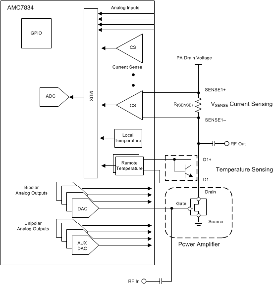 Figure 103. AMC7834 Example PA Bias System
8.2 Typical Application
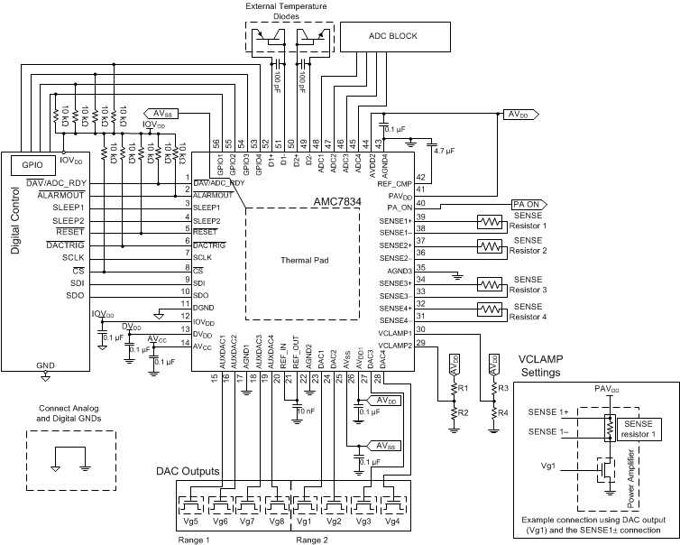 Figure 104. AMC7834 Example Schematic
8.2.1 Design Requirements
The AMC7834 example schematic uses the majority of the design parameters listed in Table 50.
Table 50. Design Parameters
| DESIGN PARAMETER | EXAMPLE VALUE |
|---|---|
| AVCC | 5 V |
| IOVDD | 3.3 V |
| DVDD | 5 V |
| AVDD | 5 V |
| AVSS | –5 V |
| 4 External unipolar inputs | ADC[1-4]: 0 to 2.5 V range |
| 4 High-Side Current Sense | Differential input of 0 to 200 mV |
| 4 bipolar DAC outputs | –4 to 1 V, –5 to 0 V, and 0 to 5 V |
| 4 unipolar DAC outputs | 0 to 5 V, 2.5 to 7.5 V |
| Remote temperature sensing | Two remote temperature diode drivers |
8.2.2 Detailed Design Procedure
Use the following parameters to facilitate the design process:
- AVCC and AVSS voltage values
- ADC and high-side current-sense input voltage range
- DAC output voltage ranges
- Remote temperature applications
8.2.2.1 ADC Input Conditioning
The AMC7834 monitoring system is centered on a single ADC core that features a multichannel input stage to a successive approximation register (SAR) ADC. The analog inputs include four external analog inputs, four internal inputs for bipolar DAC monitoring, four high-side current-sense amplifiers for PA current monitoring, two remote temperature sensors, and an internal analog temperature sensor.
The external analog inputs (ADC1 through ADC4) feature a range of 0 to Vref (Vref corresponds to either an external 2.5 V reference or the device internal reference), while the internal inputs accept a full-scale range of –5 to 2.5 V. The current-sense inputs feature a 4 to 60 V common-mode voltage range, and accept a differential input range of 0 to 200 mV. A 4.7 µF capacitor is recommended between the REF_CMP pin and the AGND4 pin. The value of this capacitor must exceed 470 nF to ensure reference stability. A high-quality ceramic capacitor, type NP0 or X7R, is recommended because of the optimal performance of the capacitor across temperature and very-low dissipation factor.
It is recommended that all external analog inputs are driven with a low impedance source to ensure correct functionality. In applications where the signal-source impedance is high, the analog inputs can be conditioned through a buffer amplifier, such as a voltage follower.
8.2.2.2 DAC Output Range Selection
The AMC7834 device has four bipolar and four unipolar DACs with programmable output ranges. The bipolar DACs feature the ranges –4 to 1 V, –5 to 0 V, and 0 to 5 V. The unipolar DACs feature the ranges 0 to 5 V and 2.5 to 7.5 V. The DAC ranges are configurable by setting the DAC range register (see the DAC Range Register (address = 0x16) [reset = 0x0000] section).
The maximum source and sink capability of the DAC internal amplifiers are listed as part of the DAC output characteristics in the Electrical Characteristics—DAC Specifications table.
The graph in the Application Performance Curve section show the relationship of both stability and settling time with different capacitive and resistive loading structures.
8.2.2.3 Temperature Sensing Applications
The AMC7834 has one local temperature and two temperature diode drivers, as well as four external analog inputs that are easily configurable to remote temperature sensor circuits. The integrated temperature sensor, remote temperature sensor, and analog input registers automatically update with every conversion. Figure 105 shows a typical setup for the two temperature diode-driver inputs. Additional noise filtering can be achieved by placing a bypass capacitor across the inputs of the remote temperature sensors. A high-quality ceramic capacitor, type NP0 or X7R, is recommended because of the optimal performance of the capacitor across temperature. See the Remote Temperature Sensors section for a details.
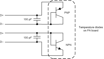 Figure 105. Remote Temperature Sensors (PNP and NPN)
Additionally, the ADC inputs can be used to accept voltage from other temperature-sensing IC circuits as shown in Figure 106. The temperature sensor use for analog input conditioning in this example is the LM50 device which is a high precision integrated-circuit temperature sensor that can sense a –40°C to +125°C temperature range using a single positive supply. The full-scale output of the temperature sensor ranges from 100 mV to 1.75 V for a –40°C to +125°C temperature range. In an extremely noisy environment, adding some filtering to minimize noise pickup may be necessary. A typical recommended value for the bypass capacitor is 0.1 µF from the V+ pin to ground. A high-quality ceramic capacitor, type NP0 or X7R, is recommended because of the optimal performance of the capacitor across temperature and very-low dissipation factor.
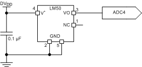 Figure 106. Temperature Sense Application With LM50
8.2.2.4 Current Sensing Applications
The AMC7834 device also features four high-side current-sense amplifiers that support common-mode voltages from 4 to 60 V and a full-scale sense voltage of 0 to 200 mV. In applications that require current sensing across a power amplifier, the SENSE± differential inputs connect across a resistor to sense small differential voltage that is proportional to current across the PA as shown in Figure 107. The current-sense conversion results are stored in the Current sense data registers. The current sensors are also configurable as closed-loop drain current controllers. See the Current Sensors section for details.
Figure 107 shows a method of separating the drain voltage from the power amplifier with a series PMOS transistor. The activation of the PMOS connects the PAVDD voltage supply to the drain pin of the power amplifier. The PMOS is driven with a voltage divider that swings from PAVDD to PAVDD(R2 / [R1 + R2]). The NMOS shown in Figure 107 is connected to the PA_ON output which controls the state of the PMOS transistor.
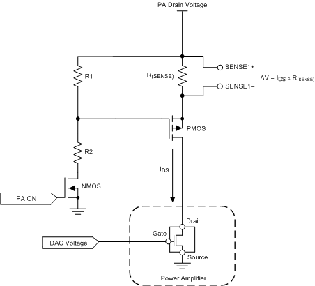 Figure 107. Current Sense (SENSE) Connections With PMOS ON and OFF
8.2.3 Application Performance Curve

| Code 0x000 to 0xFFF to within 0.5% of final value |
8.3 Initialization Set Up
8.3.1 Initialization Procedure
- Supply all voltages (PAVDD, AVDD, DVDD, IOVDD, AVCC, AVSS) and clamp inputs (VCLAMP1 and VCLAMP2). The AMC7834 does not require a specific supply sequencing.
- A 250 µs POR delay occurs after a minimum AVDD supply of 4.5 V has been applied. Do not attempt serial communication during this time.
- It is recommended to issue a hardware or software-reset.
- Wait for completion of the reset operation (at least 250 µs for a hardware reset or at least 10 µs for a software reset).
- After reset, the following conditions are met:
- The device is in open-loop mode and all DAC data registers are set to all zeros.
- All DAC outputs are set to the clamp value regardless of the SLEEP1 and SLEEP2 pin levels.
- The PA_ON signal is set to the OFF state.
- If not already done so, it is recommended to tie the SLEEP1 and SLEEP2 pins low.
- Configure the AMC7834 without the DACs leaving clamp mode.
- If the PA_ON control signal is enabled, switch the PA_ON signal to the ON state. By default, the AVSS supply must be present to enable the PA_ON signal to enter the ON state.
- Release the DACs out of clamp mode.
- Verify that the ADC has entered the READY state.
- Issue an ADC trigger signal to initiate conversion of the monitoring inputs.
After initialization the AMC7834 allows switching between open-loop and closed-loop operation. However, before switching between operating modes, it is strongly recommended to clamp the bipolar DAC outputs, stop the ADC conversion cycle, and if applicable, switch the PA_ON signal to the OFF state. To resume operation follow steps 7 through 11 of the Initialization Procedure.
9 Power Supply Recommendations
The AMC7834 supply voltage ranges are specified in the Recommended Operating Conditions table.
