ZHCSCR3C October 2012 – August 2014 DS125BR111
PRODUCTION DATA.
- 1 特性
- 2 应用
- 3 说明
- 4 简化电路原理图
- 5 修订历史记录
- 6 Pin Configuration and Functions
- 7 Specifications
- 8 Detailed Description
- 9 Application and Implementation
- 10Power Supply Recommendations
- 11Layout
- 12器件和文档支持
- 13机械封装和可订购信息
9 Application and Implementation
9.1 Application Information
9.1.1 Signal Integrity
In SAS and PCIe applications, specifications require Rx-Tx link training to establish and optimize signal conditioning settings for data rates up to 12 Gbps. In link training, the Rx partner requests a series of FIR coefficients from the TX partner at speed. This polling sequence is designed to pre-condition the signal path with an optimized link between the endpoints. Link training occurs at the following data-rates:
Table 10. Link Training Data-Rates
| PROTOCOL | MAXIMUM DATA-RATE (Gbps) | ALTERNATIVE DATA RATES (Gbps) |
|---|---|---|
| SAS | 12.0 | 6.0, 3.0 |
| PCIe | 8.0 | 5.0, 2.5 |
The DS125BR111 works to extend the reach possible by using active linear equalization to the channel, boosting attenuated signals so that they can be more easily recovered at the Rx. The repeater outputs are specially designed to be transparent to TX FIR signaling in order to pass information critical for optimal link training to the Rx. Suggested settings for the A-channels and B-channels in a SAS or PCIe environment are given in the table below. Further adjustments to EQ and VOD settings may optimize signal margin on the link for different system applications:
Table 11. Pin Mode Device Settings
| CHANNEL SETTINGS | PIN MODE |
|---|---|
| EQx | Level 4 |
| VOD_SEL | Level 7 (1) |
| VODx_DB | 0 dB (0) |
Table 12. SMBus Mode Device Settings
| CHANNEL SETTINGS | SMBus REGISTER VALUE |
|---|---|
| EQ | 0x03 |
| VOD | 110'b or 111'b |
| VODx_DB | 000'b |
9.1.2 RX-Detect in SAS/SATA Applications
Unlike PCIe systems, SAS/SATA systems use a low speed Out-Of-Band or OOB communications sequence to detect and communicate between SAS Controllers/Expanders and target drives. This communication eliminates the need to detect for endpoints like PCIe. For SAS systems, it is recommended to tie the RXDET pin high. This will ensure any OOB sequences sent from the Controller/Expander will reach the target drive without any additional latency due to the termination detection sequence defined by PCIe.
9.1.3 PCIe Applications
9.1.3.1 RXDET When Using SMBus Modes
PCIe systems use an input termination polling and detection sequence to begin the PCIe bus configuration process. When using PIN MODE configuration the RXDET pin should be left Floating to allow for this process to begin upon power-up of the DS125BR111 device. If SMBus Slave MODE configuration is required, the SMBus register write sequence in Table 13 should be initiated upon power-up of the DS125BR111.
- Pin Settings for DS125BR111 in a PCIe Application (SMBus Slave Mode)
- ENSMB = H
- RXDET = Float
- PWDN = System control (Hold HIGH until Register Write process is completed)
Table 13. PCIe RX-Detect Programming Sequence
| STEP | SMBus REGISTER ADDRESS |
REGISTER DATA (Hex) | COMMENTS |
|---|---|---|---|
| 1 | 0x08 | 0x08 | Give RXDET control to SMBus Registers |
| 2 | 0x0E | 0x04 or 0x08 | Channel A: 0x04: Auto RX-Detect, outputs test every 12 ms for 600 ms then stops; termination is Hi-Z until RX detection; once detected input termination is 50 Ω 0x08: Auto RX-Detect, outputs test every 12 ms until detection occurs; termination is Hi-Z until RX detection; once detected input termination is 50 Ω |
| 3 | 0x15 | 0x04 or 0x08 | Channel B: 0x04: Auto RX-Detect, outputs test every 12 ms for 600 ms then stops; termination is Hi-Z until RX detection; once detected input termination is 50 Ω 0x08: Auto RX-Detect, outputs test every 12 ms until detection occurs; termination is Hi-Z until RX detection; once detected input termination is 50 Ω |
| 4 | 0x06 | 0x18 | Enable SMBus register control. Register updates in Steps 1-3 are applied to high speed channels. |
- Pin Settings for DS125BR111 in a PCIe Application (SMBus Master Mode - EEPROM Configuration)
- ENSMB = Float
- RXDET = Float
- PWDN = System control (Hold PWDN HIGH until DONE = 0, EEPROM Write process is completed)
The highlighted bits for RXDET in the Table 6 show the equivalent RXDET control locations to the SMBus Register write sequence shown in Table 13.
9.2 Typical Application
SAS-3 specifications have fully specified Rx-Tx training as a means to establish and optimize signal conditioning settings at the 12.0 Gbps data-rate. The DS125BR111 works to extend the reach possible by adding active linear equalization to the channel, boosting attenuated signals so that they can be more easily recovered at the SAS-3 Rx. The outputs are specially designed to be transparent to TX FIR signaling passing this information critical for optimal link training to the SAS-3 Rx. The typical device settings used in most SAS-3 environments are EQ = Level 4, VOD_DB = 0 and VOD_SEL = 1 in Pin mode or EQ = 0x03, VOD = 111'b, and VOD_DB = 000'b in SMBus mode.
The maximum channel attenuation for a single DS125BR111 in a SAS-3 application utilizing link training is -34 dB @ 6 GHz. Other system variables such as crosstalk and channel topology can have an impact on the link extension possible using the DS125BR111.
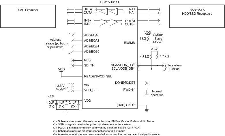 Figure 9. DS125BR111 Typical Application
9.2.1 Design Requirements
As with any high speed design, there are many factors which influence the overall performance, this section lists some critical areas for consideration and study.
- Limit the maximum attenuation to -34 dB @ 6 GHz for the entire channel.
- Utilize 100 Ω impedance traces. Generally these are very loosely coupled to ease routing length differences.
- Place AC-coupling capacitors near to the receiver end of each channel segment to minimize reflections.
- The maximum body size for AC-coupling capacitors is 0402.
- Back-drill connector vias and signal vias to minimize stub length
- Use Reference plane vias to ensure a low inductance path for the return current.
9.2.2 Detailed Design Procedure
The DS125BR111 is designed to be placed almost anywhere within the channel, maximum channel extension requires the DS125BR111 be placed with attenuation of at least 10 dB on its inputs. The device settings used in a SAS-3 environment are EQ = Level 4, VOD_SEL = 1, and VOD_DB = 0 in Pin mode or EQ = 0x03, VOD = 110'b or 111'b, and VOD_DB = 000'b in SMBus mode. This setting has proven to give the best overall SAS-3 extension for all configurations tested.
9.2.3 Application Curves
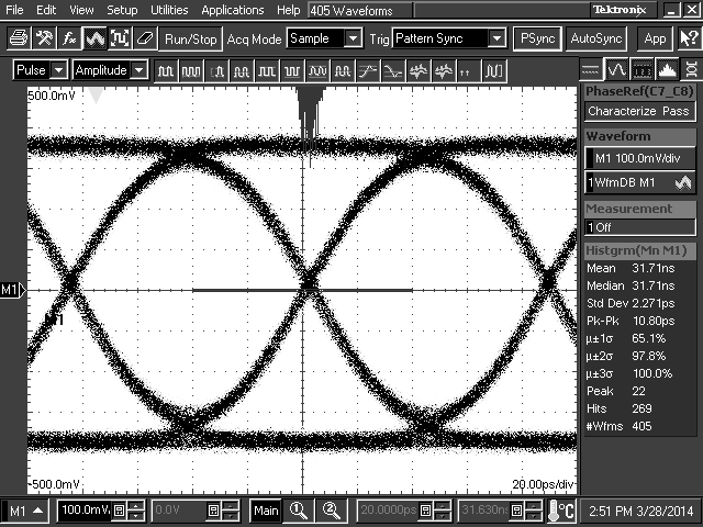
| DS125BR111 settings: EQ = 0x01, VOD = 110'b, VOD_DB = 000'b | ||