TIDU858C March   2015  – May 2021


  1.   Description
  2.   Resources
  3.   Features
  4.   Applications
  5.   5
  6. 1System Description
    1. 1.1 Binary Inputs or Digital Inputs
      1. 1.1.1 Binary Input Application Functionality
      2.      Common Specifications
    2. 1.2 Approaches to Binary Input Module Design
      1. 1.2.1 ADC Versus MCU Based Binary Input Module (BIM)
    3. 1.3 Measurement of Wide Inputs With Programmable Thresholds
  7. 2Design Features
    1. 2.1 Electrical Specifications
    2. 2.2 Block Diagram
      1. 2.2.1 Analog-to-Digital Converter (ADC)
        1. 2.2.1.1 ADS795x SAR ADC Family
      2. 2.2.2 Protection and Signal Conditioning
      3. 2.2.3 Digital Isolator
        1. 2.2.3.1 Host (SPI) Interfacing Using the ISO6741
      4. 2.2.4 DC Power Supply Isolator
      5. 2.2.5 Design Alternative: ADC With Digitally Programmable Threshold
        1. 2.2.5.1 ADS7128 SAR ADC With Programmable Threshold
        2. 2.2.5.2 I2C Interfacing Using the ISO1640 and Optional Altert Interface Using ISO7710
  8. 3Circuit Design and Component Selection
    1. 3.1 Analog-to-Digital Converter (ADC)
    2. 3.2 Input Signal Conditioning
      1. 3.2.1 Voltage Divider
      2. 3.2.2 TLV6002 Operational Amplifier
    3. 3.3 Isolated Interface
    4. 3.4 Isolated DC Power Supply
      1. 3.4.1 Reinforced Power Isolator: UCC12050 High-Efficiency 500-mW DC/DC Converter
    5. 3.5 Enhancements
  9. 4Testing
    1. 4.1 Test Setup and Connection Diagram
    2. 4.2 Test Data
      1. 4.2.1 Voltage Measurement Accuracy Testing
    3. 4.3 Test Results Summary
  10. 5Design Files
    1. 5.1 Schematics
    2. 5.2 Bill of Materials
    3. 5.3 Altium Project
    4. 5.4 Gerber Files
  11. 6References
  12.   Trademarks
  13. 7About the Author
  14. 8Revision History

Analog-to-Digital Converter (ADC)

To optimize binary input module cost profile, a 12-bit, 16-channel ADC is selected to perform binary input conversion to a host processor.
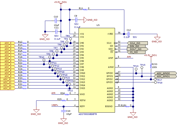
GUID-20210407-CA0I-KGT4-1NTK-4DS7QXSFLJSB-low.gif Figure 3-1 ADC Configuration for Measuring Multiple Channels

The ADC considered is the 12-bit, 16-channel, 1-MSPS, single-ended ADS7953 (see Figure 3-1). The 4–16 multichannel ADS795x family allows for auto or manual sequencing of preselected channels for the next conversion cycle. Typically at lower conversion speeds, these devices can draw 1-µA (typical) current while in power-down mode. If desired, additional signal conditioning circuitry may be applied to the MXO and AINP pins. Two programmable alarms may be utilized as well.

The ADC can operate with an external 2.5 V, ±10-mV reference that produces a clean, low-noise, and well-coupled signal. The REF5025 voltage reference with a 10-µF ceramic decoupling capacitor provides sufficient analog integrity for reliable operation.