TIDT357 November 2023
3.1 Start-Up Sequence
When VDD_CORE is supplied at 0.75 V instead of 0.85 V, power on or off sequencing between the VDD_CORE and VDDR_CORE rails become important. The sequencing requirement of ramping up the VDD_CORE rail before the VDDR_CORE rail during power on and ramping down after the VDDR_CORE rail during power off is achieved by using simple AND and OR gates along with an RC delay. The value of the RC delay depends on the value of the output discharge resistor or current sink of the converters supplying these rails. For the recommended TPS6287x-Q1 regulators, an RC delay of 7.05 ms made up with a 15 kΩ resistor and a 0.47-μF capacitor is sufficient.
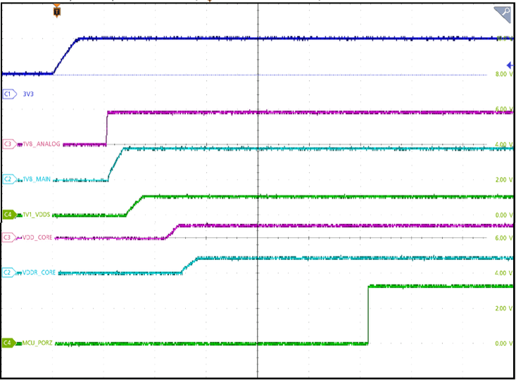
Figure 3-18 shows the power on sequencing achieved between the VDD_CORE and VDDR_CORE as well as the other AM62x-Q1 power rails. In the waveform, 3V3 represents the VDDSHVx power supply grouping, 1V8_Main represents VDDSHVy, and 1V8_Analog represents VDDA_1P8. The PMP23242 board was connected to the SK-AM62A-LP evaluation board to confirm power-up sequence.
 Figure 3-1 Start-Up Waveform