TIDT320A january 2023 – july 2023
3.3 No Load and OFF State Power Consumption
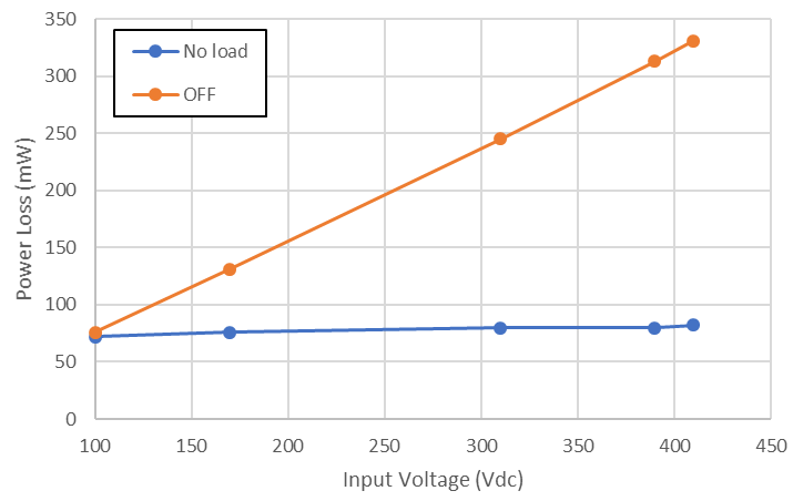
For no load power consumption, input voltage was applied with all outputs unloaded. For OFF state power consumption, input voltage was applied while the DIS pin was shorted to PGND.
 Figure 3-3 No Load and OFF State
Power Loss Graph
Figure 3-3 No Load and OFF State
Power Loss GraphTable 3-7 No Load and OFF State Power
Loss Raw Data
| Input Voltage (VDC) | No Load Input Power (mW) | OFF State Input Power (mW) |
|---|---|---|
| 100 | 72 | 76 |
| 170 | 76 | 131 |
| 310 | 80 | 245 |
| 390 | 80 | 313 |
| 410 | 82 | 331 |