TIDT304 October 2022
2.3 Thermal Images
The thermal images are shown in Figure 2-3 and Figure 2-4.
The thermal images were collected under the following conditions:
- Input: 230 VAC
- Output: 380 V, 1.3 kW
- Fan: FFB0412EN-00
- Ambient temperature: 25°C
- Time: 30 minutes
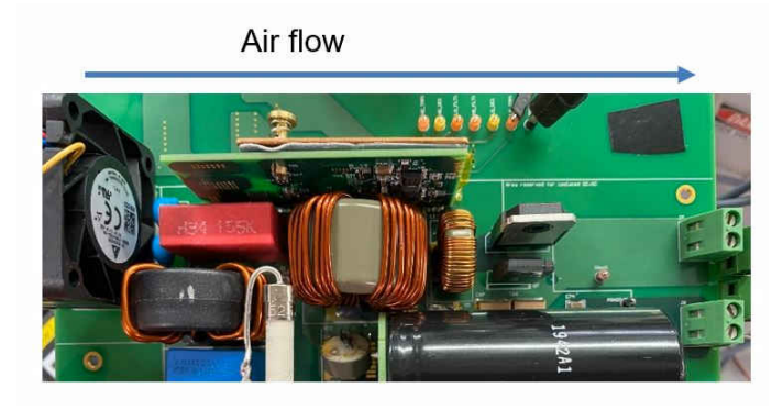 Figure 2-2 Test Setup With Air Flow
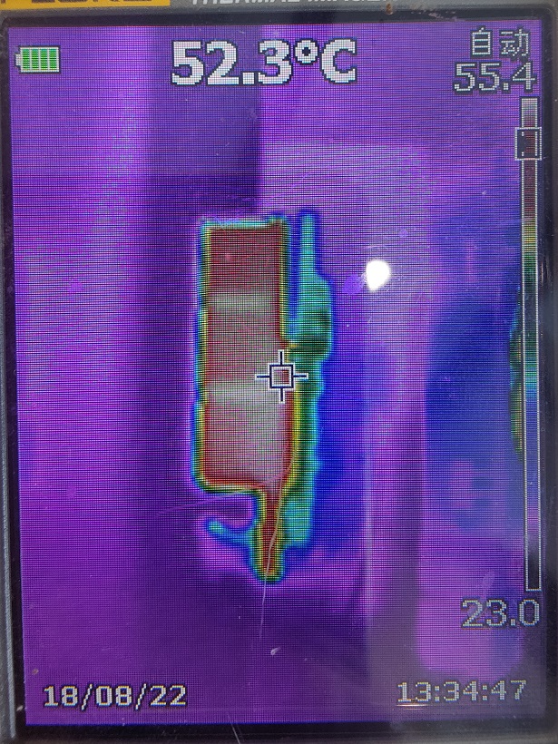 Figure 2-3 Backside of GaN FET Daughter Card
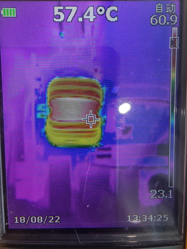 Figure 2-4 PFC Inductor
The thermal simulation conditions and results are shown in Table 2-3, Figure 2-5, and Table 2-4.
Table 2-3 Conditions
| FET | Package (× 2) | LMG3522R030-Q1 | 12 × 12 mm |
| System Power | 3-kW PFC |
| Power loss per GaN FET | 13.9 W [target RθJA = (125°C – 55°C) / 13.9 W = < 5°C/W] |
| Total power loss into heat sink | 27.8 W (2 × GaN) |
| PCB size | 40 mm × 37 mm |
| Heat sink size | 35 mm × 26 mm × 9.2 mm |
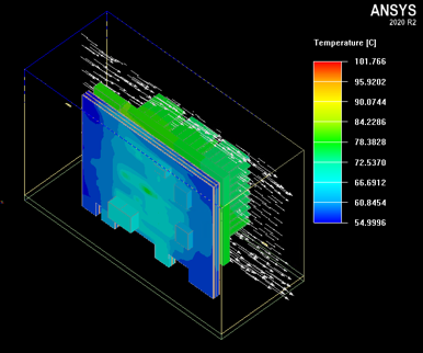 Figure 2-5 Thermal Simulation
Result
Figure 2-5 Thermal Simulation
ResultTable 2-4 Simulation Results
| Air Speed (m/s) |
TIM k W/mK (0.5-mm Thick) |
TA (°C) | P (W) | GaN 1 (°C) | GaN 2 (°C) | GaN 1 RθJA (C/W) | GaN2 RθJA (C/W) |
|---|---|---|---|---|---|---|---|
| 12 | 13 | 55 | 13.9 | 97.7 | 101.8 | 3.07 | 3.37 |
Figure 2-6 shows the heat sink specification.
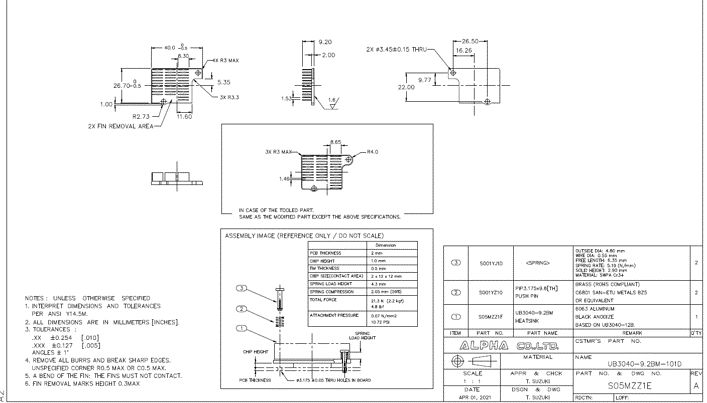 Figure 2-6 Heat Sink
Specification