• Menu
  • Product
  • Email
  • PDF
  • Order now
  • Pre-Regulated Isolated Driver Bias Supply Reference Design for Traction-Inverter Applications

    • TIDT246 September   2021


  • CONTENTS
  • SEARCH
  • Pre-Regulated Isolated Driver Bias Supply Reference Design for Traction-Inverter Applications
  1. 1Description
  2. 2Test Prerequisites
    1. 2.1 Voltage and Current Requirements
    2. 2.2 Required Equipment
  3. 3Testing and Results
    1. 3.1 Efficiency and Power Dissipation Graphs
    2. 3.2 Efficiency and Power Dissipation Data
    3. 3.3 Thermal Performance
    4. 3.4 Bode Plot
    5. 3.5 Voltage Regulation
  4. 4Waveforms
    1. 4.1 Switching
    2. 4.2 Output Voltage Ripple
    3. 4.3 Start-up
  5. IMPORTANT NOTICE
search No matches found.
  • Full reading width
    • Full reading width
    • Comfortable reading width
    • Expanded reading width
  • Card for each section
  • Card with all content


TECHNICAL REFERENCE

Pre-Regulated Isolated Driver Bias Supply Reference Design for Traction-Inverter Applications

1 Description

This pre-regulated isolated open-loop LLC transformer driver converter provides four 18-V outputs up to a total of 6 W for traction-inverter applications. The LLC topology allows the transformer to have significant leakage inductance, but a much smaller primary-secondary capacitance, which significantly reduces common-mode current injection through the bias transformer. The boost pre-regulator is designed to provide 7.5 W to the LLC converter, which can support a maximum of 6-W output.
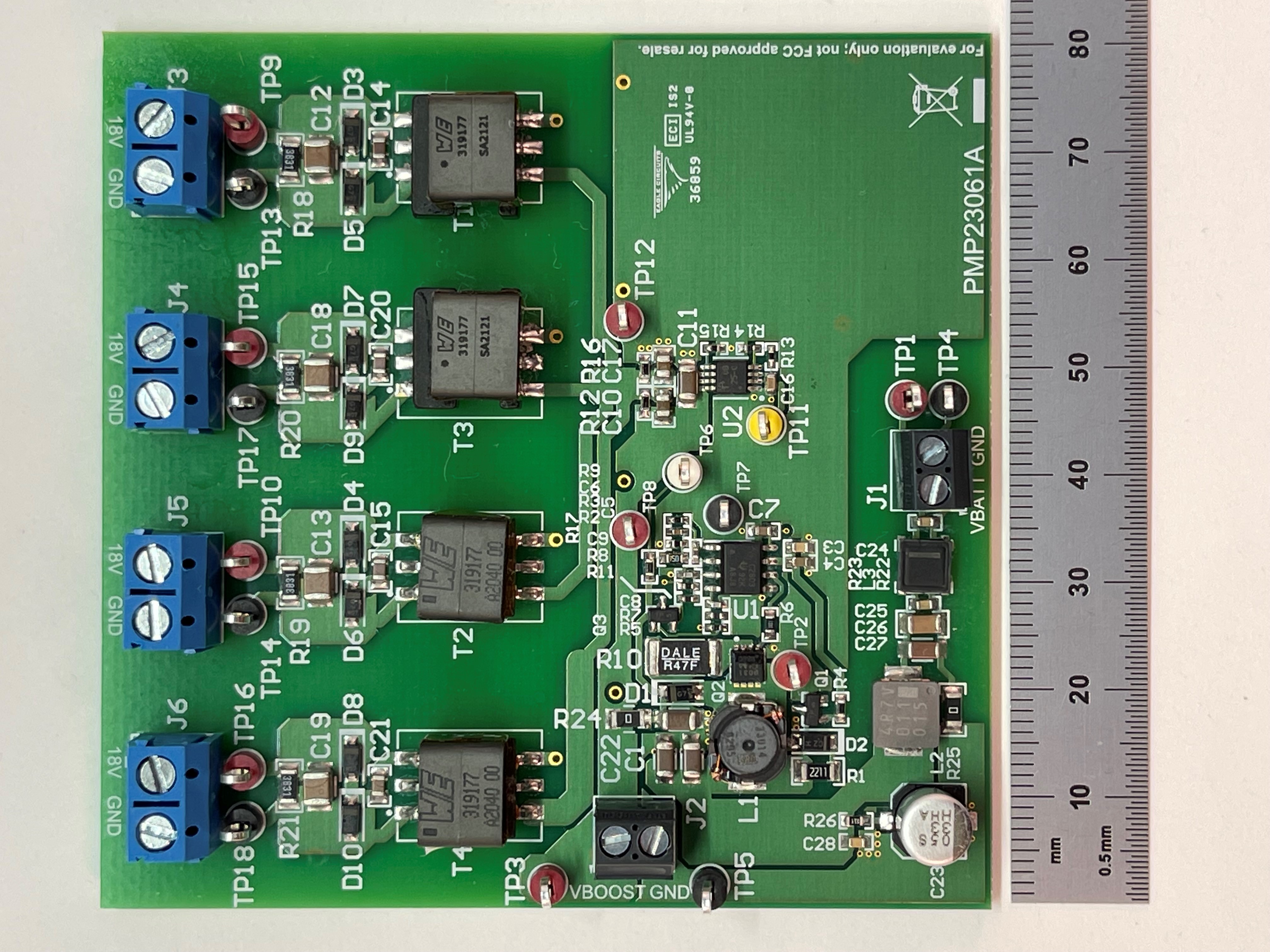
GUID-20210720-CA0I-NNVR-LN86-L4SJV1QC9K0P-low.jpgFigure 1-1 Top Photo

2 Test Prerequisites

2.1 Voltage and Current Requirements

Table 2-1 Voltage and Current Requirements
Parameter Specifications
Input voltage range 6 V–28 V
Output voltage and current 4 × 18-V rails, 1 × 167 mA, 3 × 56 mA, 6 W maximum
Switching frequency Boost: 300 kHz, LLC: 1 MHz
Isolation Yes
Topology Open-loop LLC transformer driver with boost pre-regulator

2.2 Required Equipment

  • Resistive loads
  • Power supply capable of 30 V, 10 W minimum
  • Oscilloscope and probes
  • Digital multimeters

3 Testing and Results

3.1 Efficiency and Power Dissipation Graphs

The efficiency of the boost converter and the open-loop LLC were measured separately. For the boost measurements the LLC was disabled by shorting the DIS/FLT pin of the UCC25800-Q1 (TP11) to GND and a resistive load was applied across the connector labeled VBOOST (J2). Efficiency curves were measured for inputs of 6 V, 12 V, 24 V, and 28 V.
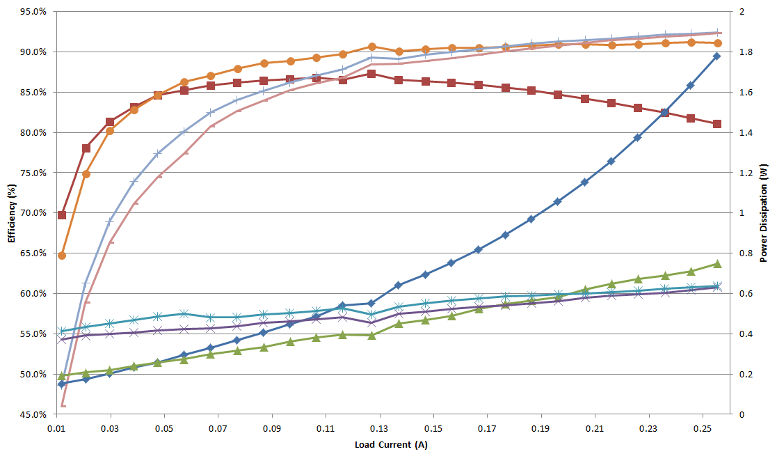
GUID-20210720-CA0I-X8WC-DV8C-BCBBBCTQC3DB-low.pngFigure 3-1 Boost Efficiency and Power Dissipation

The LLC measurements were taken with a regulated 30 V applied at the connector labeled VBOOST (J2) and with the boost input (J1) disconnected.
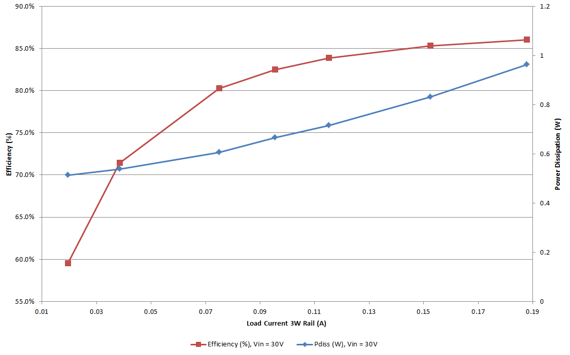
GUID-20210720-CA0I-CRRK-2VS6-RTCNDVNFLSRZ-low.pngFigure 3-2 LLC Efficiency and Power Dissipation

3.2 Efficiency and Power Dissipation Data

The efficiency and power dissipation data for the boost and LLC stages is shown in the following tables.

GUID-20210720-CA0I-KHXB-LJHL-SFWDPP0NK0MB-low.png Figure 3-3 Boost Converter Efficiency, 6 VIN
GUID-20210720-CA0I-SPZW-1STF-NPB5TBSGFKTN-low.png Figure 3-4 Boost Converter Efficiency, 12 VIN
GUID-20210720-CA0I-883B-G1Z1-DW2M8QTLV7MD-low.png Figure 3-5 Boost Converter Efficiency, 24VIN
GUID-20210720-CA0I-SJJV-BQCZ-WSTZPW7WL71Q-low.png Figure 3-6 Boost Converter Efficiency, 28 VIN
GUID-20210720-CA0I-04FX-FX48-XLFMR4HPC23H-low.png Figure 3-7 LLC Converter Efficiency, 30 VIN

3.3 Thermal Performance

The following thermal image shows the board running with 6 VIN and 6 W being drawn from the 18-V LLC outputs (3 × 1 W and 1 × 3 W).

GUID-20210720-CA0I-HV0G-JCBK-9MCSXL5MLWDF-low.jpgFigure 3-8 Top Thermal Image

3.4 Bode Plot

The loop stability of the boost converter is shown in the following plot. The plot was obtained with the LLC converter disabled and a resistive load applied across J2.

GUID-20210720-CA0I-SDVG-S7KK-RDF9JRDQXRJ9-low.jpgFigure 3-9 Loop Stability, 12 VIN, 250-mA Load

3.5 Voltage Regulation

The voltage regulation of the LLC converter outputs is shown in the following figures.

GUID-20210720-CA0I-PHQ2-VG7H-CBDB0RXXFT08-low.pngFigure 3-10 3-W Rail Regulation Graph
GUID-20210720-CA0I-DK2B-81T1-1MVVZMPBPT1N-low.pngFigure 3-11 3-W Rail Regulation Table
GUID-20210720-CA0I-VSPX-QTXJ-HGXZK2FT3X3B-low.pngFigure 3-12 1-W Rail Regulation
GUID-20210720-CA0I-P0HP-9CD9-XN9ZL9BWVCGM-low.pngFigure 3-13 1-W Rail Regulation Table

The cross regulation was measured to showcase the effects of varying load on the other outputs of the LLC converter. The 3-W rail (Vo3W) and one of the 1-W rails (Vo1W3) were varied while the other 2 rails (Vo1W1 and Vo1W2) were held constant.

GUID-20210720-CA0I-Z0KR-BKLH-RLL2DZN3K4PT-low.pngFigure 3-14 Cross Regulation Table

4 Waveforms

4.1 Switching

The switching behavior of both converters is shown in the following figures. As in previous sections, the two converters were evaluated separately.

GUID-20210720-CA0I-SRF6-TM9S-FC5FRKCXGWFF-low.pngFigure 4-1 Boost Converter Switch Node, 6 VIN, Light Load
GUID-20210720-CA0I-WC8R-KJP2-SQ6WZ2PC8LKL-low.pngFigure 4-2 Boost Converter Switch Node, 6 VIN, Maximum Load
GUID-20210720-CA0I-THGW-MHPZ-BVC4JTNGLWHL-low.pngFigure 4-3 Boost Converter Switch Node, 28 VIN, Light Load
GUID-20210720-CA0I-G8VL-G1WD-81PPR7TBHMCX-low.pngFigure 4-4 Boost Converter Switch Node, 28 VIN, Maximum Load
GUID-20210720-CA0I-0XKT-HGTD-QQKMT1PNFPBG-low.pngFigure 4-5 LLC Converter Primary Side Switch Node, 30 VIN, No Load
GUID-20210720-CA0I-PSWQ-T5MF-LWNVC741QTW2-low.pngFigure 4-6 LLC Converter Primary Side Switch Node, 30 VIN, 50% Load
GUID-20210720-CA0I-PBXR-1P3C-X8HLKLRKF2FL-low.pngFigure 4-7 LLC Converter Primary Side Switch Node, 30 VIN, Max Load
GUID-20210720-CA0I-JQGM-TP6L-QGSW0KTBHQZX-low.png Figure 4-8 LLC Converter Secondary Side Resonant Capacitor, 30 VIN, Max Load

4.2 Output Voltage Ripple

The output voltage ripple of each converter is shown in the following figures.

GUID-20210720-CA0I-JQMC-ZG2J-RB0NWFFV2M0P-low.pngFigure 4-9 Boost Converter Output Ripple, 6 VIN, Maximum Load
GUID-20210720-CA0I-WNF9-NRRB-96QFMRNDNBLB-low.pngFigure 4-10 Boost Converter Output Ripple, 28 VIN, Maximum Load

The LLC output ripple was measured on the 3-W rail to show the worst-case ripple.

GUID-20210720-CA0I-DSKF-HWR9-MQZTFRRM0XHV-low.pngFigure 4-11 LLC Converter Output Ripple, 30 VIN, Maximum Load

4.3 Start-up

The start-up behavior of each converter is shown in the following figures. The boost converter start-up was measured on controller enable, the controller was disabled by shorting the COMP pin to GND. VOUT is shown in yellow.

GUID-20210721-CA0I-LN2N-1KTD-TP7HKPMLQGTP-low.pngFigure 4-12 Boost Converter Start-up, 13.5 VIN, Maximum Load

For the LLC converter, a 3-W output (yellow) and a 1-W output (blue) are shown.

GUID-20210720-CA0I-MN7F-NTHV-JP2ZK7BSQ2Z6-low.png Figure 4-13 LLC Converter Start-up, 30 VIN, No Load
GUID-20210720-CA0I-VNGC-6R2G-9KPCHHRGGZR4-low.png Figure 4-14 LLC Converter Start-up, 30 VIN, 50% Load
GUID-20210720-CA0I-G8DX-HF4N-3HGJCNCPVF7L-low.png Figure 4-15 LLC Converter Start-up, 30 VIN, Maximum Load

IMPORTANT NOTICE AND DISCLAIMER

TI PROVIDES TECHNICAL AND RELIABILITY DATA (INCLUDING DATASHEETS), DESIGN RESOURCES (INCLUDING REFERENCE DESIGNS), APPLICATION OR OTHER DESIGN ADVICE, WEB TOOLS, SAFETY INFORMATION, AND OTHER RESOURCES “AS IS” AND WITH ALL FAULTS, AND DISCLAIMS ALL WARRANTIES, EXPRESS AND IMPLIED, INCLUDING WITHOUT LIMITATION ANY IMPLIED WARRANTIES OF MERCHANTABILITY, FITNESS FOR A PARTICULAR PURPOSE OR NON-INFRINGEMENT OF THIRD PARTY INTELLECTUAL PROPERTY RIGHTS.
These resources are intended for skilled developers designing with TI products. You are solely responsible for (1) selecting the appropriate TI products for your application, (2) designing, validating and testing your application, and (3) ensuring your application meets applicable standards, and any other safety, security, or other requirements. These resources are subject to change without notice. TI grants you permission to use these resources only for development of an application that uses the TI products described in the resource. Other reproduction and display of these resources is prohibited. No license is granted to any other TI intellectual property right or to any third party intellectual property right. TI disclaims responsibility for, and you will fully indemnify TI and its representatives against, any claims, damages, costs, losses, and liabilities arising out of your use of these resources.
TI’s products are provided subject to TI’s Terms of Sale (www.ti.com/legal/termsofsale.html) or other applicable terms available either on ti.com or provided in conjunction with such TI products. TI’s provision of these resources does not expand or otherwise alter TI’s applicable warranties or warranty disclaimers for TI products.
Mailing Address: Texas Instruments, Post Office Box 655303, Dallas, Texas 75265
Copyright © 2021, Texas Instruments Incorporated


Texas Instruments

© Copyright 1995-2025 Texas Instruments Incorporated. All rights reserved.
Submit documentation feedback | IMPORTANT NOTICE | Trademarks | Privacy policy | Cookie policy | Terms of use | Terms of sale