-
High-Voltage Buck Converter Reference Design for E-Motorcycle BMS Applications
High-Voltage Buck Converter Reference Design for E-Motorcycle BMS Applications
Description
This non-isolated buck converter provides a fixed output of 12 V at 400 mA for BMS applications. It operates over an input voltage range of 50 VDC–150 VDC after a start-up greater than 40 V. Operating in Discontinuous Conduction Mode (DCM), this converter utilizes the UCC28730 controller, which is referenced to the switch node. It offers high efficiency and low cost in a compact form factor.
 Figure 1-1 Board Photos, Top and Bottom Views.
 1 Test Prerequisites
1.1 Voltage and Current Requirements
| Parameter | Specifications |
|---|---|
| Input voltage range | 50 V - 150 V, after > 40 V start-up |
| Output voltage and current | 12V ±3%, 400 mA maximum |
| Switching frequency | Variable, 83 kHz max |
| Isolation | No |
| Controller features | Valley switching, frequency dithering, internal 700-V start-up switch, overcurrent and overvoltage protection |
1.2 Required Equipment
Resistive load (resistor decade box), 5 W minimum
Power supply, adjustable, 0 V–200 V and 0.25 A minimum
Oscilloscope and probes
Digital multimeter
2 Testing and Results
2.1 Thermal Images
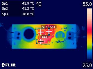
This thermal image shows the operating temperature of the top side of the board with 120 VDC input and 12 V at 400-mA output at room temperature and no air flow.
 Figure 2-1 Top-Side Thermal Image, 120-VDC Input, 12 V at 400-mA Output
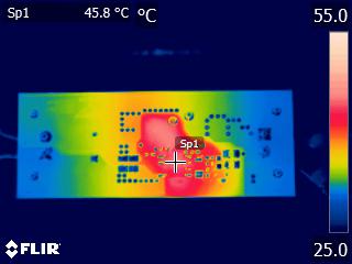
This thermal image shows the operating temperature of the bottom side of the board with 120-VDC input and 12 V at 400-mA output at room temperature and no air flow.
 Figure 2-2 Bottom-Side Thermal Image, 120-VDC Input, 12 V at 400-mA Output.
 2.2 Efficiency and Power Dissipation Graphs
The following figure displays the efficiency and power dissipation of the converter at input voltages of 60 VDC, 90 VDC, 120 VDC, and 150 VDC.
 Figure 2-3 PMP22557 Efficiency, VOUT = 12 V.
 2.3 Efficiency and Power Dissipation Data
Efficiency data is shown in the following tables.
 Figure 2-4 Efficiency Data for VIN = 60 V, 90 V
 Figure 2-5 Efficiency Data for VIN = 120 V, 150 V.
 2.4 Voltage Regulation
The following graph displays the measured output voltage at input voltages of 50 VDC and 150 VDC.
 Figure 2-6 PMP22557 Voltage Regulation