SSZTCM0 june 2015 TPS544B20 , TPS544C20

Power density requirements for power supplies in cloud infrastructure end equipment like servers, Ethernet switches, base stations, and storage attach boxes is increasing. In response, the use of integrated MOSFET (Metal Oxide Semiconductor Field Effect Transistor) DC/DC converters for high-current POL (Point of Load) rails that have been traditionally served by PWM (Pulse Width Modulated) controllers with external MOSFETs has become mainstream. Also, the need to perform advanced tasks for high-performance processors and FPGAs like adaptive voltage scaling (Vout adjustment on the fly based on the processor operational profile to optimize power loss) has become important. Furthermore, power supply designers are increasingly focusing on eliminating external components, increasing reliability and preventing failures before they happen.
Today, TI offers the TPS544C20 and TPS544B20 power converters that combine these two very powerful ideas into a single IC. On the one hand, they have integrated MOSFETs with enormously high 30A and 20A current-carrying capabilities, and on the other hand, they feature PMBus™ control.
What is ‘PMBus’ and why is it such a valuable power feature? PMBus, which stands for ‘power management bus,’ is the “remote control” of power management. PMBus control encompasses the powerful idea that you can control and program power management devices with software commands on the fly. This is not achievable in pure analog design where you would set the device behavior and select the resistors and capacitors at the design phase. With the PMBus protocol, a controlling processor can change things like the switching frequency, current limit and output voltage. PMBus can also provide telemetry, which is reading things like IC temperature and current so that the processor can monitor the power system dynamically.
The idea of PMBus owes its origins to the popular I2C bus developed in the early 1980’s. The I2C bus, which stands for inter-IC (integrated circuit), was a general-purpose bus to control and monitor any electronic system. It was a simple bus protocol replacing the many proprietary protocols that existed at the time. From the I2C bus, came the SMBus protocol or the System Management Bus, defined in 1995. SMBus differed slightly from I2C as it added packet error checking, making it more robust. SMBus was used for PCs and servers but It was soon realized by the industry that the power management needs of systems is best served by a common protocol and set of standards, which culminated in the definition of PMBus control. PMBus, while using the SMBus as a physical layer, sets up the protocol for power management, replacing several propriety protocols.
TI’s SWIFT™ TPS544C20 and TPS544B20 are the industry’s first 4.5V to 18V, 30A DC/DC converters with integrated FETs and PMBus digital interface. To make it easy for an engineer to design with these products, we added support in WEBENCH® Power Designer. From within the WEBENCH tool you can exercise many of the PMBus commands and see the immediate impact, helping you quickly analyze and prototype the design.
As an example, let’s change the output voltage of a controller in real-time using PMBus commands. Let’s say you want to throttle down the performance of a microprocessor in a power-sensitive application, like a laptop, to save on battery life. As you know, power dissipation in a microprocessor is proportional to C V 2 f . Power dissipation depends on the square of voltage, so a reduction in voltage has an enhanced impact on reducing power. The microprocessor can dynamically issue a PMBus command to the power converter to reduce the output voltage via the PMBus bus. This Vout transition command is executed by the TPS544C20 or TPS544B20 to change its Vout. The design steps are illustrated below.
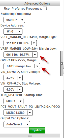
I created a design with the TPS544C20 for nominal output voltage of 3.3V delivering an output current of 20A. Input voltage is 4.5V to 5.5V. In the advanced options I set the PMBus command Vref Margin Low to -16.67%, and the operation margin to “Margin Low” for lowering the output voltage (Figure 1).
 Figure 1 Set PMBus Commands in the
“Advanced Options” WEBENCH Panel.
Figure 1 Set PMBus Commands in the
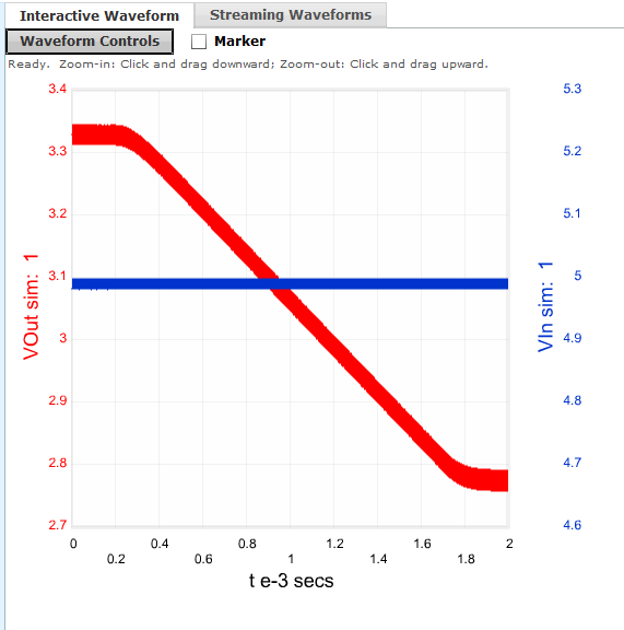
“Advanced Options” WEBENCH Panel.This sets up the TPS544C20 to transition Vout from the nominal value of 3.3V to 2.75V, which is 16.67% lower. You can simulate this effect in WEBENCH Power Designer using the online “Vout Transition” simulation (Figure 2).
 Figure 2 Vout Transition
Simulation.
Figure 2 Vout Transition
Simulation.If you zoom into the output voltage waveform, you will see the output voltage ripple along with the average Vout, which transitions from 3.3V to 2.75V. The operating value in the Op Val section indicates all variables for the new Vout.

Watch a video on how to create a design and run the Vout transition simulation.
Get a copy of the exact WEBENCH design I used in this video (it was created using the new “Share with Public” feature).
Try your hand at creating a PMBus system power design in WEBENCH Power Designer using the PMBus features and analyze the design with online SPICE simulations.
I’d love to hear from you—please drop your comments below.