SSZTCH4 july 2015 LM5119
In part 1 of this blog, I discussed the necessity of interleaving the four phases of a synchronous buck to minimize input/output voltage ripple and improve thermal performance. You can further enhance thermal performance by following some key layout guidelines to ensure that the power is dissipated evenly across all four phases.
All four phases must have the same exact L-C output filter; you should select these filters to minimize the DC resistance (DCR) (inductor) and equivalent series resistance (ESR) (capacitor) losses. The LM5119 will share current between the four phases evenly, provided that both the shared traces between the controllers and the feedback traces are noise-free. The four switch nodes are the noisiest on the board, and to avoid noise coupling must be avoided. You can accomplish this by routing noise-sensitive traces along the edge of the board. Figure 1 highlights how the compensation pins of both ICs are tied together using an internal layer (shown in yellow) along the edge of the board.
 Figure 1 COMP Pins of U1 and U2 Tied
Together on an Internal Layer
Figure 1 COMP Pins of U1 and U2 Tied
Together on an Internal LayerFigure 2 shows the VOUT trace being carefully routed along the edge of the board to avoid the switch nodes. If possible, you should route this trace on the same internal layer as the COMP pins and surround the trace with GND copper pours to ensure noise immunity.
 Figure 2 Feedback Trace Routed along
the Edge of the Board to Avoid Noisy Switch Nodes
Figure 2 Feedback Trace Routed along
the Edge of the Board to Avoid Noisy Switch NodesThe power stage must be laid out to ensure that the noise is contained while having enough copper to withstand the power requirement. Make sure that the input capacitors are as close as possible to the drain of the high-side MOSFET and the source of the low-side FET. This will minimize switch-node ringing. Next, minimize the switch node so that it is only as big as necessary to carry the high currents. Keep all of the power-stage components on the top side of the board to contain noise to one side, so that it is not communicated to other layers.
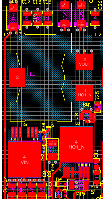
Figure 3 shows the top-layer power stage for one of the phases of the automotive multi-phase synchronous buck power module reference design (PMP10979). The power flow starts from the bottom with input capacitors (C6, C7), then to the high-side and low-side FETs (Q1, Q3), followed by the inductor (L1) and ending with the output capacitors(C17, C18).
 Figure 3 Top-layer Placement of
Power-stage Components
Figure 3 Top-layer Placement of
Power-stage ComponentsI used four layers for this design, with 2oz of copper to ensure good heat transfer. The customer requirements entailed that I only mount components on the top side of the board. To reduce board size further, you can place the ICs on the bottom layer, directly under the two phases they control. This will also help to reduce the length of key traces such as feedback and COMP. The top layer should have most of your IC signals, as well as copper pours for switch nodes, input and output voltages, and GND. Reserve the second layer for GND only and run multiple vias to dissipate the low-side FET heat quickly and efficiently. Reserve the third layer for VIN, VOUT and any other IC signals. The fourth layer is all GND.
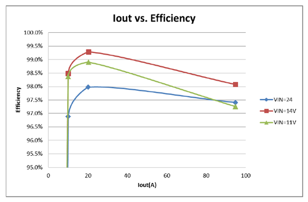
The overall benefit of interleaving the four phases and having an optimized layout is that it will increase the efficiency of the power supply. Figure 4 shows the high efficiency measured from PMP10979, with various input voltages.
The automotive and industrial industries are booming, and demands on the non-isolated synchronous bucks are becoming more strenuous. Using a multiphase design in order to reduce the losses will also reduce part counts, decrease the board size and provide better thermal performance.
 Figure 4 Efficiency of PMP10979 With Different Input
Voltages
Figure 4 Efficiency of PMP10979 With Different Input
VoltagesAdditional Resources:
Read more Power Tips blogs