SSZTCG8 july 2015 INA199 , INA210 , INA282
In previous installments of this series, I discussed implementation alternatives and how those decisions affect and are affected by device parameters. In this post, I’ll explain how device parameters as well as system factors can affect the achievable accuracy.
To understand how accurate a measurement we can achieve, we first need to understand the sources of potential errors. Here is a list of two types of error sources – note that this is not an exhaustive list, but rather highlights some of the main sources:
Amplifier-related Error (Noise) Sources:
- Input offset voltage (VOS).
- VOS drift.
- Common-mode rejection ratio (CMRR).
- Power-supply rejection ratio (PSRR).
- Gain error.
- Gain-error drift.
Nonamplifier Error Sources:
- Printed circuit board (PCB) layout.
- Shunt-resistor tolerance and drift.
- Gain-setting passives tolerance, matching and drift.
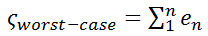
The worst-case accuracy is a simple linear summation of all error sources, e, shown in Equation 1:
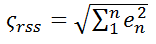
It is statistically improbable that all errors are maxed at the same time, so a more probable accuracy equation would be a root-sum-square of the error sources, shown in Equation 2:
First, let’s consider the external error sources. The VSENSE that the amplifier sees is what is across the input pins, which will be different than what a designer may experience if measuring across the resistor. Ideally VSHUNT = VSENSE, but parasitics and trace etch will cause this not to be true. A Kelvin connection will minimize the PCB parasitic-error contribution.
When it comes to shunt-resistor tolerance and drift, there will be a trade-off between the cost you are willing to pay and the required performance for the application. The shunt-resistor temperature drift is one of the main error sources over temperature, unless you choose a costly resistor. High-precision (0.1%), low-drift (50ppm/°C) resistors on catalog distribution sites cost somewhere between US$4.00 and US$8.00 in 1,000-unit quantities.
The error contribution of an operational amplifier’s external circuitry is eliminated using a current-shunt monitor due to its integrated, matched, low-drift gain-resistor networks. The effects of these on-chip networks are factored into the error contributions of the current-sense amplifier itself.
When it comes to amplifier error sources, you will need to make similar trade-offs on precision versus cost. It is important to review the operating conditions of each of the parametric specifications listed in the datasheet and compare those to your actual operating conditions. For this discussion, I will focus on two of the main error contributors: input offset voltage and gain error.
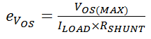
The input offset voltage will be the dominant error source at low VSENSE levels. If you simplify and assume that VSENSE = VSHUNT = ILOAD x RSHUNT (no parasitic error contribution), then the error contribution of VOS is calculable using Equation 3:
Let’s look at two different current-shunt monitors, the INA199 and INA210, to see how VOS will affect the error. The INA199 datasheet lists the VOS(MAX) as 150µV, while the INA210 is 35µV. Table 1 shows the respective error contributions using a current value of 1mA and a 1Ω shunt resistor.
| INA199 | INA210 | |
|---|---|---|
| VOS(MAX) | 150µV | 35µV |
| VOS error | 15.0% | 3.5% |
If you are measuring low current values that will result in low VSENSE values, it is critical to minimize VOS to minimize the error. As VSENSE grows relative to VOS(MAX), this error contribution is minimized. If VSENSE is 1,000 times the value of VOS, then the error contribution is 0.1%. On the other end of the spectrum is when VSENSE is much greater than VO. The main error contribution will be the gain error. In most datasheets, this is specified as a flat percentage, and the contribution is a straightforward percentage adder.
Let’s see how these two errors contribute to a total error, again assuming that they are the only two error sources. Figure 1 shows how the linear sum as well as the root-sum-square method of error calculation work for the INA199 and INA210.

Here, the offset voltage is the major error source when VSENSE is low, and gain error dominates when VSENSE is high relative to VOS.
My analysis has simplified the error calculations to two primary sources. However, current measurement accuracy is a very complex subject with many moving parts that need to be traded off against each other to maximize performance under specific operating conditions. One of the key elements for a more thorough analysis is temperature. The temperature drift will affect multiple specifications, including shunt-resistor value, offset voltage and gain error. Using a current-shunt monitor that has zero drift, including the INA210 or INA282, will help minimize the offset drift contribution.
Additional Resources
- Read the datasheets for the INA210, INA199 and INA282 current-shunt monitors.
- Read this “Current sensing tutorial” article series on EE Times.
- Watch our training series on current-sense amplifiers.
- Check out related TI Designs reference designs: