SSZTCE8 July 2015 LP2951
This post is co-authored Aditya Ambardar.
Designers often face the challenge of protecting power sources from abrupt shorts or continuous high draw of current, because loads can behave unpredictably in many industrial and automotive applications. Low-dropout (LDO) regulators often power these loads, but have no built-in protection. In this post, we’ll discuss a concept to effectively increase the LDO regulator’s impedance, thus protecting the input from unpredictable load conditions.
Figure 1 shows the basic internal functionality of the single-channel LP2951. On the right-hand side, you can see that there are two resistors connected in sequence. When this device is connected for a 5V regulated output, VTAP is tied directly to feedback, and sense is connected directly to output. Note that this produces a voltage divider from the output voltage to ground, with the reduced voltage being sent to the error amplifier. This feedback loop is what keeps the output at 5V.
 Figure 1 Functional Diagram for the
LP2951
Figure 1 Functional Diagram for the
LP2951Using the two resistors inside the device is just one way to configure it. By using an external voltage divider, it’s possible to choose any voltage within the device’s output range. The process for doing this is described in the data sheet, but to keep a specific voltage on the output is simple. By using an external circuit, the current limit of this part can be reduced from the factory setting to a user-selectable level. For example, let’s take a look at how you would use this technique to reduce the output voltage if the current draw is getting too high.
 Figure 2 A Current-limiting Circuit for
the LP2951
Figure 2 A Current-limiting Circuit for
the LP2951Figure 2 shows the full circuit used. Since the input current will be the same as the output current, you can place the shunt resistor on the input side to directly monitor the output current without affecting the output voltage.
On the right side, the input feeds into a shunt resistor and then directly to the VIN pin. With no current flowing, the voltage across Rshunt will be zero and VEB for the PNP transistor will also be zero, which means that the transistor will be off and no current will flow through RC. The added PNP circuit will have no impact on the voltage divider on the left side of the diagram, and the LP2951 will work normally. See the equation example below.
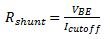
Once some current starts to flow through Rshunt, it will develop a voltage and eventually will turn on the PNP transistor because VBE > VF and the transistor will conduct. The transistor will force additional current into the feedback node and the output will change accordingly. The shunt resistor value is calculated by deciding on a desired cutoff current, Icutoff, and using Equation 1.
The added voltage at feedback will make the LP2951 “think” that it is outputting more than the required voltage, and the output will reduce in voltage. The beauty of this circuit is that the shunt resistor value selects the output current limit. A larger resistor will produce the threshold voltage at a lower current and will roll off the output voltage sooner. The value of RC allows designers to choose the final rolloff value at the output by controlling the amount of current added to the node.
Any values of R1 and R2 that meet this ratio will work, but to reduce power consumption, values in the 10 to 100 kΩ range are best. Choosing R2 to be 10kΩ, R1 is easily calculated as 30.49kΩ. Using a standard value of 33kΩ will not result in much error (VOUT = 4.977V). See Equation 2:
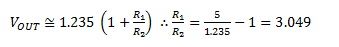
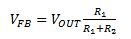
In order to force the output to a lower voltage, you need to trick the device into thinking that the output is increasing, which means that you need to force a higher voltage at the feedback node. The amount of voltage that you will need to add is determined by speculating that the output reaches the lower voltage, and calculating the difference between the feedback node voltage at 5V and the selected lower voltage. The feedback voltage at 5V will be 1.235V (by definition) and the voltage at the lower voltage will be defined by Equation 3:
The difference between the two voltages is what you must add to the node to force the output to the lower voltage, or . To add the desired voltage to the feedback node, additional current must pass through that resistor. Equation 4 calculates the amount of current required:

The value of RB is not important because very little current will pass through it in this circuit. We recommend a value of 10k, but any value from 1k to 100k would be acceptable.
Now that the desired collector current has been found, you can calculate the final component value. RC is calculated using Kirchhoff’s voltage law, drawing a loop through the base-emitter junction of the transistor and the shunt resistor. See Equation 5:
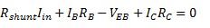
You can assume that IBRB is approximately zero, so the only remaining unknowns are VEB and RC. The data sheet of the selected transistor will include VEB, and you can easily calculate RC after that.
The LP2951 gives designers the capability to control its output with more than a simple resistor network. By using active components properly, you can link the output to the input current and protect sensitive circuitry. This circuit is certainly not the only solution available, but it is a simple one that anyone can test out and use.
Additional Resources
- Download the LP2951 datasheet.
- Read the application note, “LDO Noise Demystified.”
- Check out all of TI’s LDOs.