SSZTC34 october 2015 CC1310 , CC2630 , CC2650 , HDC1010 , HDC1050 , TPL5100 , TPL5111 , TPS22860 , TPS61291
In my previous blog post, I discussed the importance of long battery life in wireless sensor nodes and a specific duty-cycled implementation. In this post, I’ll expand on some of the power-topology considerations for these wireless sensor nodes.
In some wireless sensor nodes, you have to provide a well-regulated operating voltage for various integrated circuits. Perhaps a high-precision analog-sensing component needs a voltage that doesn’t drift, or a component in the sensor node requires a higher voltage than what the battery can provide. In addition, as voltage drops off near the end of the battery’s life, that battery’s usable range is shortened. Adding a well-designed boost converter can provide the missing link to achieving long battery life in wireless sensor nodes.
In a duty-cycled wireless sensor node, nearly the entire sensor node powers down completely during the off state. For optimal battery life, this would include any power management. When transitioning to the on state, the boost converter begins normal operation, providing a well-regulated voltage rail to the analog-sensing circuitry as well as to the Sub-1 GHz wireless microcontroller (MCU). If the efficiency of the boost converter is very high at the on-state currents, then the battery-life reduction caused by the efficiency loss of the DC/DC converter will be minimal. The addition of a boost converter will also increase the battery’s useable voltage range. You won’t need to make compromises between battery life and a well-regulated voltage rail.
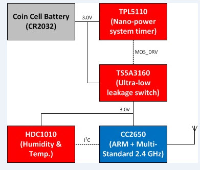
A TI Designs reference design for humidity and temperature sensor nodes (TIDA-00484) demonstrates an optimized method to provide a well-regulated 3.3V rail to the analog-sensing and wireless MCU in a duty-cycled sensor node. Figure 1 is a system block diagram for the Humidity & Temp Sensor Node for Sub-1GHz Star Networks Enabling 10+ Year Coin Cell Battery Life reference design. The boost converter used in this example has a built-in bypass mode, which is critical for extending battery life. Figure 2 shows a typical application circuit for the TPS61291 boost converter.
 Figure 1 Block Diagram for the
TIDA-00484 Reference Design
 Figure 2 TPS61291 Boost Converter
Typical Application
Figure 2 TPS61291 Boost Converter
Typical ApplicationIn this topology, the nanopower system timer controls both the ultra-low-leakage load switch and the boost converter bypass mode. In the off state, the boost converter is set to bypass mode, which connects the battery directly to the load switch, while bypassing the boost inductor to reduce losses. The quiescent current of the boost converter during this time is typically 15nA. The load switch opens during the off state, which disconnects the humidity sensor and wireless MCU from the output of the boost – and effectively, the battery.
During the on state, the nanopower system timer sets the boost converter to normal boost operation and closes the load switch, which connects the analog sensing and wireless MCU to the now-regulated 3.3V voltage rail. The addition of the regulated voltage rail enables the sensor node to more fully deplete the battery and use sensors that may have minimum voltages higher than the battery voltage.
This reference design optimizes overall system battery life, since the bypass mode of the boost converter, the nanopower system timer and the ultra-low-leakage load switch reduce the off-state average current to tens of nanoamps, which is lower than most typical MCU shutdown modes. In addition, the wireless MCU and humidity sensor used in this reference design are extremely low power, which reduces the on-state average current to less than 5mA. Since the sensor measurement and wireless data transmission only take about 30ms to complete, the estimated system battery life is greater than 10 years (measuring once per minute).
When used in a duty-cycled architecture with a nanopower system timer, this boost converter makes wireless sensor nodes a practical reality for various sensor types. With system battery life longer than the typical shelf life of the batteries themselves, this TI Designs reference design shows how you can use a differentiated boost converter to implement wireless sensor nodes for many applications.
Additional Resources:
- Review my last post about achieving long battery life in wireless sensor nodes.
- Read this Industrial Strength blog post about the proliferation of sensor nodes in the Internet of Things (IoT).
- Find out more about TI's building automation system solutions