SSZTC14 october 2015 TPS22915 , TPS22946
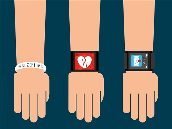
In just five years, wearables have gone from being essentially non-existent to an integral part of daily life. As the popularity of these devices continues to grow, their feature set also becomes more diverse. What started out as a simple way to track your steps has turned into a wrist-worn data center listening to every heart beat and analyzing every e-mail. These complex features mean additional design challenges for engineers.
When it comes to designing a wearable, you must consider many requirements including size, cost, and performance. In this blog, I will focus on two issues that an integrated load switch can address:
- Minimizing leakage current from subsystems and other components.
- Protecting systems from inrush current and other current spikes.
How to Minimize Leakage Current from Subsystems and Other Components
One of the biggest challenges for wearables is their small form factor. This not only makes layout difficult, but presents an even bigger issue as the size of the battery is constrained. In an effort to extend battery life, designers must consider every source of leakage in the system. The highest leakage often comes from subsystems such as the Bluetooth® circuitry or the heart rate monitoring signal chain, which are only on during certain modes of operation. Even when disabled, circuitry such as DC/DCs and linear regulators (LDOs) can exhibit high leakage. By inserting a small-form-factor load switch such as the TPS22915 between the subsystem and the power source, you can significantly reduce the leakage current (Figure 1).
 Figure 1 Comparison of Leakage Current with and without a Load Switch
Additionally, the TPS22915 incorporates quick output discharge (QOD), which ties the output to ground when the switch is turned off. This guarantees that the downstream subsystem or additional circuitry is completely off resulting in the lowest possible leakage.
How to Protect Systems from Inrush Current and Other Current Spikes
With customers demanding new features and designers being forced to reduce cost and save board space, it is very easy to put a low priority on protection. However, by using an integrated load switch in your design, you can add protection against inrush current and other current spike events.
Inrush current control is a common problem for wearables. When turning on a subsystem, it is possible for the input rail to sag from a quickly charging load capacitance (Figure 2). All TI load switches address this issue by controlling the rise time of the load switch output voltage and limiting the inrush current to ensure that the subsystem sees a controlled current on the input rail (Figure 3).
 Figure 2 Inrush Current from Turning on a Subsystem
 Figure 3 Slew Rate Control Provided by a Load Switch
Additionally, TI load switches such as the TPS22946 incorporate protection features such as current limiting. Current limiting ensures that a constant current is delivered to the system despite any excessive current that would otherwise by pulled by a subsystem or some external circuitry. This is especially critical for devices using USB as a source to recharge the battery.
Adding an integrated load switch to your design can extend your device’s battery life by reducing leakage current and can improve reliability by protecting against current spikes. With a TI load switch, you get these benefits with minimum impact to board space or cost. Start integrating a load switch to your design today and check out our additional resources below!
Additional Resources:
- Learn more about TI’s load switch portfolio
- Read the following TI application notes: