SSZTBO9 January 2016
In the previous post in this series, an equation was derived to describe the ratio of the Nth RSET resistor in Figure 1 below.
 Figure 1 Current Sink Network
That equation, again, is as follows:
So, what can be said about Equation 1? First of all, for an MIN ratio of 1, the corresponding MRN ratio will also be 1, as would be expected. Second, for values of MIN greater than 1, notice that the two terms of the denominator of Equation 1 take on different signs. This means that depending on certain physical quantities involved (Kn, RSET1, VREF), MRN can become arbitrarily large. Thus, this region should be avoided, instead favoring the MIN ≤ 1 region; that is, by ensuring that ISINKN is less than or equal to ISINK1 for all N.
Notice that allowing the denominator of the root term in Equation 1 (the Kn, RSET1, VREF product) to become large results in a 1:1 linear relationship between MRN and MIN in the limit. Ultimately, the range of usable values that VREF and RSET1 can take on to increase this product are going to be limited by the headroom required for the sink; though it is worth noting that for a fixed ISINK1 value, increasing VREF requires an increase in RSET1 as well. The final variable in the product, Kn, is the process transconductance of the MOSFET and can be maximized through device selection. The effect of Kn on the linearity of the MRN, MIN relationship (across five decades of Kn values) is illustrated in Figure 2 below.
 Figure 2 Resistor Ratio vs. Current
Ratio across Process Transconductance
Figure 2 Resistor Ratio vs. Current
Ratio across Process TransconductanceThe process transconductance is so named due to its dependence on carrier mobility, oxide permittivity, and oxide thickness (μ, εox, tox)—all material and process properties:
However, it is also dependent on the W/L ratio of the device, so in general larger devices will result in increasingly linear behavior in Equation 1. While most datasheets will not include Kn, it can be calculated from a common datasheet parameter, the forward transconductance, often listed as gm or gFS:
Recall that the drain current equation for an NMOS operating in the saturation region is:
Neglecting channel length modulation and rewriting the terms of Equation 4:
This result can be substituted into Equation 3 and ultimately solved for Kn:
Thus, using Equation 7 it is possible to select optimal MOSFET devices for the bias network. Further, having obtained this value, it can be utilized in Equation 1 to calculate (more accurately) required RSETN resistor values to produce desired ISINKN currents.
It is important to note that Equation 1 tends to overestimate the RSETN resistance in the MIN ≤ 1 region; that is, it results in currents that are lower than the desired value. However, the ideal transistor case (MIN=MRN) will always underestimate the RSETN resistance in this region. Thus, calculating these two values will ultimately bound the exact value required. Consider two randomly chosen NFETs, N-channel MOSFET A and N-channel MOSFET B, as represented in Table 1, which have listed gFS values of 5.5A/V2 (at ID=9A) and 15A/V2 (at ID=31A), respectively. Suppose these are used to implement an MIN ratio of ¼; the corrected RSETN and MRN ratios are calculated using Equation 1 (along with some straightforward design values) in Table 1 below.
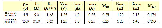
|
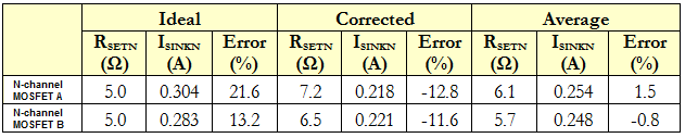
Using the conditions listed above for the N-channel MOSFET B, Figure 3 displays the results of a TINA-TI simulation of the circuit in Figure 1 implemented with RSETN values calculated from the ideal case (5Ω under these conditions), the corrected case (Equation 1), and the average of these two.
 Figure 3 Sink Current vs. Drain Voltage
for Ideal, Corrected, and Average RSETN Values
Figure 3 Sink Current vs. Drain Voltage
for Ideal, Corrected, and Average RSETN ValuesThe results for simulations using both the N-channel MOSFET A and N-channel MOSFET B with the three RSETN values (as described above) are summarized along with corresponding percent error calculations in Table 2 below.
|
Ultimately a single feedback device can be used to derive a bias network of arbitrary values so long as certain conditions are met: particularly that the current in the primary feedback driven leg is the largest in the network, and the proper headroom is maintained in each leg. Thus, from a single voltage reference, a bias network is established.