SSZTBO1 February 2016 LM2775 , LM2776 , MAX232 , TPS65150
Life was simple when I first became interested in electronics. Components were so big I could solder them without a microscope. Switching converters switched at a whopping 25 kHz, digital circuits all used a 5-V supply voltage and all the computers I came across used the RS-232 serial interface to communicate.
The RS-232 standard specifies that a logic 0 is represented by voltages between 5 V and 25 V, and a logic 1 by voltages between –5 V and –25 V. My problem was that although almost all the components on my boards needed only a 5-V supply, I still had to generate those two extra rails for my RS-232 interface.
Then I came across the MAX232. This device was an inspired product, combining two line drivers, two line receivers, and a positive and negative charge pump. With that bad boy running off a single 5-V supply, I could generate the additional supply voltages I needed and transmit and receive serial data.
Charge pumps are useful little DC/DC converters that use a capacitor to store energy instead of an inductor. They can be found in dedicated charge-pump devices such as the LM2775/LM2776 devices, as auxiliary rails in LCD bias supplies such as the TPS65150, or as external circuits put together from a couple of diodes and a couple of capacitors.
Generally speaking, charge pumps are:
- Simple, often comprising no more than two diodes and two capacitors.
- More forgiving than DC/DC converters.
- Good for output currents in the tens of milliamps range (but not so good for currents much higher than 250 mA).
- Less efficient than inductor-based DC/DC converters, unless they are unregulated and running open -loop.
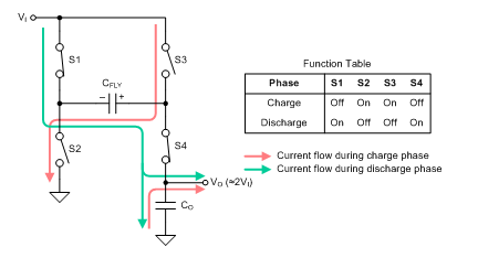
Figure 1 is a simplified circuit diagram of an unregulated charge pump. The charge pump operates in two phases:
- During the charge phase, switches S1 and S4 are open and switches S2 and S3 are closed. Current flows through S2 and S3 and charges the flying capacitor, CFLY, up to a voltage of VI.
- During the discharge phase, switches S1 and S4 are closed and switches S2 and S3 are open. The negative terminal of CFLY is now at VI and the positive terminal (which is VI volts higher) is now at 2VI. Current flows from VI through the flying capacitor CFLY and switches S1 and S4. Charge is transferred from CFLY to the output capacitor, CO, to generate an output voltage approximately equal to 2VI.
 Figure 1 Simplified Charge-pump
Block Diagram (Voltage Doubler)
Figure 1 Simplified Charge-pump
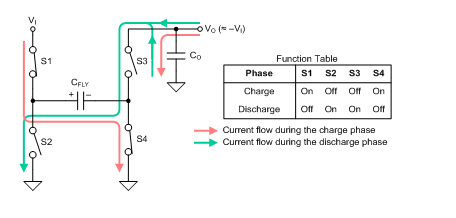
Block Diagram (Voltage Doubler)You can rearrange the same four components (S1, S2, S3 and S4) to generate a negative output voltage equal to approximately –VI (see Figure 2).
 Figure 2 Simplified Charge-pump Block
Diagram (Voltage Inverter)
Figure 2 Simplified Charge-pump Block
Diagram (Voltage Inverter)The circuit just described works well, but its output voltage is unregulated. Such a simple circuit is sufficient is some applications, but a charge pump with a regulated output is much more useful.
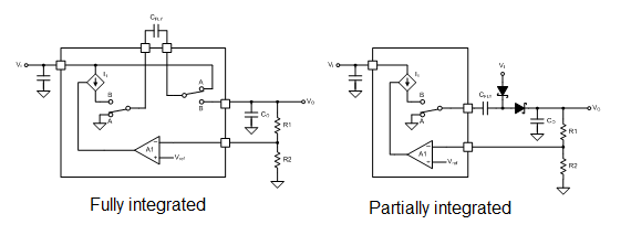
The usual way to regulate the output voltage of a charge pump is to put an adjustable current source, I1, in series with switch S1, or S2 in the case of an inverting charge pump (see Figure 3). The error amplifier, A1, adjusts the value of I1 until the output voltage is correct. Under steady-state conditions, I1 is exactly twice the value of IO.
 Figure 3 Different Charge-pump
Integration Levels
Figure 3 Different Charge-pump
Integration LevelsNote that a simple, regulated voltage doubler can only regulate its output voltage in the range of VI to 2VI. It cannot generate output voltages lower than VI. There are some fancy tricks you can do to make a buck-boost charge pump, but these kinds of devices are more complicated than the one shown in Figure 3.
Additional Resources:
- Find help deciding between a charge pump, inductor-based converter or LDO.
- Browse the charge pump portfolio.
- Learn more about “The Forgotten Converter” in this white paper.